- Ask a related questionWhat is a related question?A related question is a question created from another question. When the related question is created, it will be automatically linked to the original question.
This thread has been locked.
If you have a related question, please click the "Ask a related question" button in the top right corner. The newly created question will be automatically linked to this question.
Hi Ti experts,
We now use INA146 for Battery voltage measurement when the battery is charged during the battery formation process.
Problem: There will be a ESD phenomenon of up to 500V(sometimes 1kV) between the positive side of battery and the GND of 220V input.
Question: So what the maximum voltage can the input side of INA146.
Do you have relevant test verification data?
What should we do to protect INA146 from ESD? It that work to connect the TVS device in parallel with the input of INA146 to ground.
Hi Gary,
this thread might interest you:
Kai
Hi Gary,
So what the maximum voltage can the input side of INA146.
Since INA146 is designed prior to 2000s, its ESD input pin protection may not be rated to the current ESD standard. I do not have these ESD figures either, and I have to request the ESD specification, if we have any data on file. Please give me a couple days and see if I am able to find these specification.

What should we do to protect INA146 from ESD?
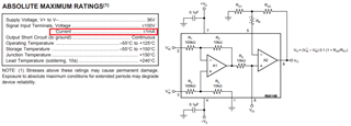
Kai has provided a great link about passing ESD events. In any case, you have to place bidirectional TVS at the input of INA146 terminal (GND line is not required). In addition to ESD voltage clamp, it is necessary to limit the current at its input terminal. Per the specification in INA146, the input current shall be limited below +/-1mA.
If the TVS protection diodes are able to clamp and dissipate the ESD energy during ESD events (I do not have the ESD rating requirements for the application), it is not difficult to pass this test, even if INA146 is only rated approx. 500V in HBM specification (and you want to perform 1kV or higher HBM ESD level tests). The key is to have an adequate external TVS protection (voltage clamp) and current limiting protection at its input terminals.
Please also find the previous E2E reply in INA146 ESD input protection topics.
If you have additional questions, please let us know.
Best,
Raymond
Hi Gary,
I have confirmed that the INA146U passes 1500V HBM and 1000V CDM. So INA146U's input should withstand the nominal ESD strikes (up to 1.5kV-HBM) without further protection (at an IC level).
At system level as shown at the input terminal as the block diagram is drew, I am not sure that Li+ battery is able to withstand the ESD strikes without damages in a long run. This is something that you need to consider. In theory, the battery cell should be able to handle the ESD strike. But it is also possible that the absorbed ESD energy may partially shorten some of the battery's internal layer, then it is not a good practice. Anyway, this is a risk that is required to be considered in order to have good design.
If you have other questions, please let us know.
Best,
Raymond
Got it. Now the problem is that INA146 is damaged by the ESD from Battery positive lug. So do you have some reference design of ESD protection for INA146. Thx.
Hi Gary,
have you read what Raymond has written? ESD can also destroy your lithium ion battery! So you should urgently change the design of your battery lug, if it is permanently producing damaging ESD. And if it's not a person which injects ESD but a misconstructed battery lug you could even suffer from ESD of much higher energy compared to HBM ESD. Or you could even suffer from Burst (EFT) and Surge.
Raymond did also tell you that you need to mount a TVS between the inputs of INA146. I would start with a 1.5KE15A. Mount it not too close to the INA146 but close to the battery lug, to the source of ESD.
But mounting a TVS is only half the truth. In my given links I have mentioned that the ESD current must be shunted away from the printed circuit board and its sensitive circuitry. So shunt the ESD current by the help of a 10nF/1kV cap (Y-cap for safety) from the negative terminal of TVS (GND2) directly to earth, protection earth or functional earth. But do it close to the battery lug and not too close to the INA146 or printed circuit board. The idea is to shunt the ESD current entirely arround the sensitive circuitry and to not allow it to enter the printed circuit board. Read again my links.
An additional protection against ESD, Burst and Surge is to have the INA146 circuit on a printed circuit board containing a solid ground ground plane. Also, have all the connectors of signals leaving or entering the board at one edge of the board, so that no EMI current can flow across the board. Read again my links.
Kai