This thread has been locked.

If you have a related question, please click the "Ask a related question" button in the top right corner. The newly created question will be automatically linked to this question.

LM193-N: Circuit explanation

Part Number: LM193-N
Other Parts Discussed in Thread: LM193, TLV3201, TLV2371, LM311, LM111, SN6505B, OPA381

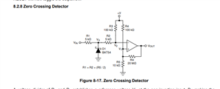
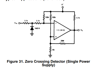
Please explain the following circuits. Why are resistors chosen the way they are chosen? one of the circuit has a pull-up and the other doesn't. Kindly cover that point also in explanation.

  • Hi Mohammed,

    the upper circuit has a comparator with a push-pull output stage not needing a pull-up resistor and the lower circuit has a comparator with a open collector output stage needing a pull-up resistor.

    The advantage of the circuit (when being designed properly !) is that even when the input voltage "Vin" goes negative, the -input of comparator will never see a negative going input voltage because of the clamping diode and the 100k / 5k1 voltage divider. Assume the supply voltage is +24V and the input voltage "Vin" causes a voltage drop of -0.65V across the diode. Then the 100k / 5k1 voltage divider produces a voltage of +24.65V / 105k1 x 5k1 = +1.20V higher than the -0.65V across the diode, resulting in +0.55V at the -input of comparator. The voltage at the -input of comparator is always higher than +0.55V and by this the common mode input voltage range of LM193 is never violated.

    Kai

  • Thanks Kai for the great explanation.

    Mohammed, 

    Just wanted to add that we also have an app note on this, albeit a slightly different design than the ones you posted: Zero crossing detection using comparator circuit

  • VG1, VG2, VG3 are 3 phase AC source, with an input signal voltage varying from 1V to 2.9V. VG4, VG5, VG6 are 100mv(1000Hz) added to introduce noise.

    I'm calculating zero crossing with reference to line 2(Reference) in the given circuit. The intention of the circuit is to detect line voltage zero crossing. i,e, Line voltage of V1 and V2.

     I observe that at low value input signals, there is false triggering. and also, if i increase noise signal amplitude there is false triggering. I tried using TLV2371. Also, i tried using TLV3201(Comparator), results are worse. Kindly help with what is happening.

    1.How do i add hysteresis to this circuit to avoid false triggering at low value signals? 

    2. also what value of diode to be added and why?

    3.Also please explain what if i don't add a diode?

    4. Is there a better and simpler way to do it?

    Zero crossing detection using comparator circuit(3201).TSC

  • Hi Mohammed,

    please tell more about your application. What is the nature of VG1, VG2 and VG3? Has it anything to do with mains voltage and have safety issues to be considered?

    Kai

  • yes, safety is considered. after considering all safety, i'm receiving 3 phases-3wire(Delta connection). Application is to calculate phase angle. Im trying to capture zero-crossing of the line voltage, not phase voltage. then i will take that input as interrupt in controller in mcu. I'm having trouble with the zero-crossings.

    Note: I missed to add ground connection in simulation file, Please find the below file.

    0131.Zero crossing detection using comparator circuit(3201).TSC

  • I am closing this post since there are two open threads on the same topic.

    Chuck

  • Thanks mate, Circuits works.

    Couple of questions:

    1. If i reduce Input voltage , Till what point i can reduce ? what parameters to vary ? Because @ Vin= 0.7V, Im getting false trigger. Also please do give detail design parameters.

    2. Why did you choose dual supply ? 

    3. I have space constraint, I'm having a supply of +5V. Is there a way to do with +5V ?

    4. If there is different (better) comparator, Kindly suggest the same.

  • Mohammed

    Thanks again for your post.  I noticed that you responded to this thread, so I will close the other so we don't need to manage both.

    My suggestion would be to ac-couple the lines going to the comparator and add pullup resistors to 2.5V to level shift as shown in the attached file.

    This would eliminate the need of creating the split supply.  4571.moh_tlv3201_ac_couple.TSC

    Chuck

  • Thanks for the suggestion. But as i mentioned i have space constraint on my board, since +2.5V is on ac side, i will have to choose a separate isolated power supply.  And as mentioned above, my signal input max is +2.9V, which would false trigger output in many ways. Need to look at some other option

    1. BDW, why is level shifting needed ? Does it has something to do with common mode voltage ? if yes, please explain. Also if i use diode at inputs, how will it help the circuit ?

    2.Also, I asked a couple of question in the above reply to Kai. Can i get some knowledge on them. 

  • I was thinking you could create the 2.5V from the 5V.  But to answer your direct question, the comparator has ESD clamping diodes to GND on the inputs.  From the datasheet, each input has abs max rating of -0.5V and -0.2V recommended range for the TLV3201.  So if level shifting isn't preferred, you will need to externally clamp with diodes to be operating within specification.

    Chuck

  • Kai's split supply solution also solves the problem and was a very good option but since you are challenged to create the additional supply voltages, I am offering you alternatives.  For completeness, if you had option for split supply, I would have recommended changing comparators to LM311 which allows for split supply input and single supply output.

    Chuck

  • I will need to consider all possible options. Can you give me a circuit covering my input signal (1V - 2.9V) using LM311.. Let me go through that option also. (Lm311 does not qualify for industrial grade temp +125C, Suggest an alternate along with circuit)

  • LM111 and LM211Q are both qualified to 125C

    I modified Kai's circuit to include the LM111 instead of TLV3201.  I presume this would be better since whatever is downstream of the comparator probably needs single supply logic levels.  the output pullup can be to any voltage required downstream.

    Hope this helps.

    Chuck

  • Sorry, looks like the attach didn't take.

    4571.moh_LM111.TSC

  • Couple of final questions:

    1. Please do give out explanation on how you chose 100K for added hysteresis?

    2.ALso why 10K are present at both inputs?

    3.also shed some light on Voltage offset and how will it have an impact for slow moving signal (50 ~ 60 Hz)?

    4.are there any changes to be done in circuit?

  • Please do explain the circuit component selection.

    1.Why C1 and R2 are chosen in that manner ?

    2.Why +2.5(Pull-up) is given through 100K to each input? what if i don't pull up the signals? Is there a way to do without a pull up.

    3. Impact of offset in this type of circuit ?

  • R3 (10k)

    It is a common trick with amplifiers to match impedance on the inputs so bias current doesn't create additional input offset. 

    By adding hysteresis to minimize the impact of noise in the system, input offset of the comparator is minimized.

    I do not believe additional changes would be required.

    Chuck

  • Ac Coupling.TSC

    Couple of questions on this type of circuit.

    Please do explain the circuit component selection.

    1.Why C1 and R2 are chosen in that manner? Please provide calculation on selecting these components

    2.Why +2.5(Pull-up) is given through 100K to each input?

    3. what if i pull up the signals other than +2.5V?

    4. Is there a way to do without a pull up.

    5. Can i use resistor divider to generate +2.5V? will that be a good idea? or what do you recommend.

    6. Impact of offset in this type of circuit? 

  • Hi Mohammed,

    when you have a bigger circuit and have to generate the pseudo ground at various places, you may need more board space then when using a bipolar supply voltage generated from a DC/DC converter, especially if you need low pass filtering in the pseudo ground generation down to very low frequencies. Also consider the additional caps you need in the signal path for the AC coupling when using a single supply.

    A true signal ground offered by the bipolar supply voltage, on the other hand, offers huge advantages over a pseudo ground which can only absorb very limited currents and can only be low pass filtered for a limited frequency range.

    I would first build the circuit for a bipolar supply voltage and then, in a second step, adapt it to a single supply voltage powering, if still needed at all.

    Kai   

  • Thanks for sharing the knowledge.

    1. I have asked a couple of questions in the above post, please do answer them too if you're handling this post.

    zero crossing_LM111.TSC

    2. For the above-mentioned file I will be using SN6505B to generate both positive and negative supplies, any precautions I need to take ?

  • Hi Mohammed,

    I do not "handle" this post. I'm not a TI's employee but only a guest and contribute here from time to time just for fun.

    For the DC/DC-converter I meant something like that:

    https://eu.mouser.com/c/power/dc-dc-converters/isolated-dc-dc-converters/isolated-dc-dc-converters-through-hole/?q=dc%20dc&input%20voltage%2C%20nominal=5%20V&output%20power=1%20W&output%20voltage-channel%201=5%20V&output%20voltage-channel%202=-%205%20V&NewSearch=1&sort=pricing

    Don't forget to mount Pi-filters at the inputs and output, though.

    Kai

  • Hi Mohammed,

    Here are my comments to your questions:

    1.Why C1 and R2 are chosen in that manner? Please provide calculation on selecting these components

    the caps are there to ac couple the inputs and resistors are there to limit some of the current going into the inputs. 

    2.Why +2.5(Pull-up) is given through 100K to each input?

    the 2.5V pull up is there so that the voltages seen at the inputs of the comparator is within the input voltage range; otherwise, the inputs would be negative. 

    3. what if i pull up the signals other than +2.5V?

    we would recommend you pull to a voltage that is within the input voltage range. +2.5V was chosen because you can create it from the +5V supply. 

    4. Is there a way to do without a pull up.

    if you do not want to use a pull up, you can try using an external diode clamp so that when the input goes negative, it would clamp the inputs within the input voltage range. 

    5. Can i use resistor divider to generate +2.5V? will that be a good idea? or what do you recommend.

    yes you could generate the +2.5V from the 5V supply using a resistor divider. 

    6. Impact of offset in this type of circuit? 

    offset could affect the timing of the circuit and shift the output. however, with hysteresis you can minimize this effect by reducing the effect of noise in this system. 

  • Thanks a lot, much appreciate it.

    AC zero_crossing.TSC

    Kindly review the circuit.

    VG1, VG2, VG3 values vary from 0.5V ~ 3V.

    VG4, VG5, VG6 are 100mV, 10Khz noise source.

    Let me explain what has evolved since then, the actual circuit board has parts till OPA381. So, i had to modify my circuit,. Since 100K value resistors are used, it will limit the negative half. Now my actual circuit starts after OPA381, so I'm taking input from the output of OPA381. Also, I'm using AC hysteresis in the circuit

    As seen in the waveform result, I'm detecting Zero crossing at one side of the Line voltage; I'm thinking to consider this detection for zero-crossing. Will it be, Ok?

    I changed and adjusted values of resistors and cap, the circuit seems to be working fine somehow for 0.5V ~ 3V.

    But i don't know exactly how the circuit works? Let me tell a scenario, if i vary R4 less than 2.2K, let's say around 1K, and input voltage (VG1, VG2, VG3) is around 0.5V, there will be false triggering. Is it because of the noise signals (VG4, VG5, VG6) which is around 100mv, and there is no room for proper hysteresis? What happens at Vac threshold node,.....

    it's all messed up in my brain. Please explain how the circuit operation is happening with input voltages (0.5V ~ 3V) and impact of AC hysteresis at least with some nodal values

  • Hi Mohammed,

    Since this is going beyond the use of the forum, I am going to reach out to you offline so we can discuss this further. I will be closing this thread as well as your other post as they are related. Please accept my friend request so I can message you offline.

    Thanks,

    Chi

  • Ok! thanks. yes, i have accepted it

  • Thanks, closing this post.