This thread has been locked.
If you have a related question, please click the "Ask a related question" button in the top right corner. The newly created question will be automatically linked to this question.
Hi TI
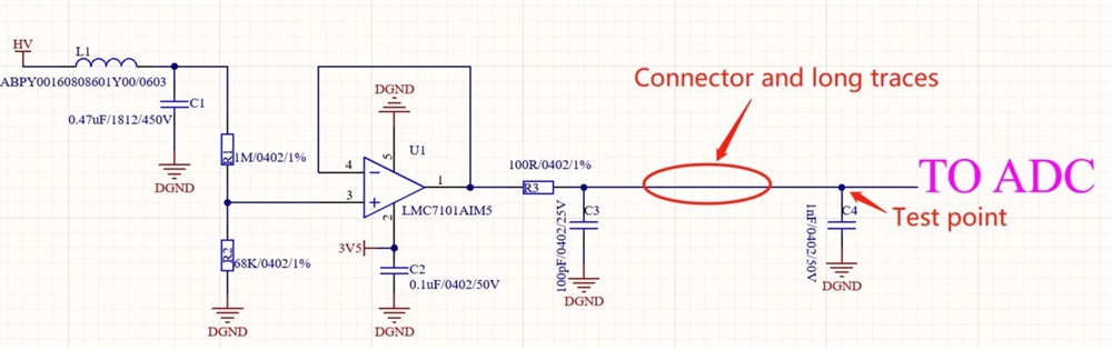
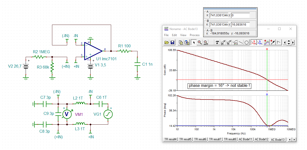
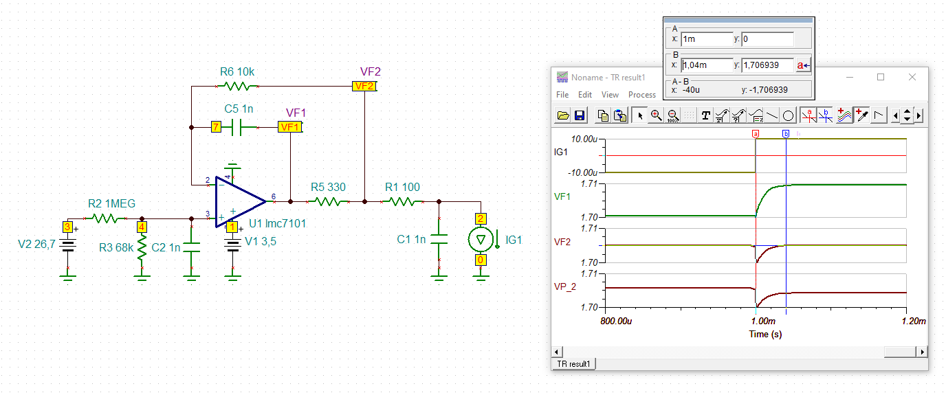
Circuit function: The operational amplifier (LMC7101AIM5/NOPB/SOT23-5/TI) is designed to follow the circuit to sample ADC and monitor the change of voltage.
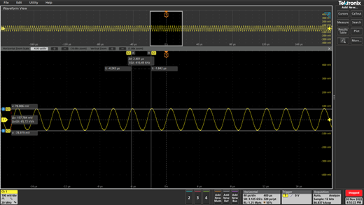
Phenomenon: during the test, it is found that the output voltage signals of the 10 prototypes of the R&D prototype are normal (normal in normal temperature and high temperature environment tests); However, in the small batch stage, all the output signals of the op amps in the 10 prototypes showed oscillation waveforms (see the figure below), and the higher the temperature, the higher the amplitude of oscillation. The circuits and PCBs of the two batches are identical.
The customer did the ABA test, and the abnormal phenomenon followed the bad film. Please help analyze the cause.
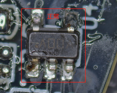
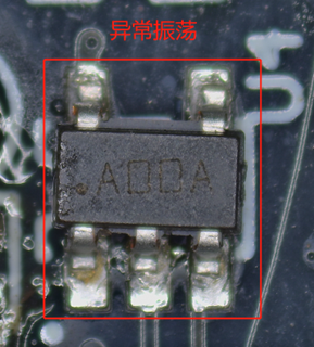
In addition, we found that the silk screen of the defective products was inclined. Will this happen in our production stage?
Hey Rain,
Could you please provide a picture of the sticker from both orders of the devices?
Best,
Jerry
Rain,
Could you also please provide a picture of the sticker from both orders of the devices?
Best,
Jerry
Hi Rain,
unfortunately, your circuit isn't stable:
Applying the dual feedback method can enhance the stability:
Kai
Hi Kai
Thanks for your support;
1. Why are (- IN) and - IN and (+IN) and+IN in the circle not directly connected? The purpose of doing this is not understood, please help guide?
2. What is the role of L2 and L3 in the figure?
Customer's circuit changes:
The customer changed C4 in his schematic diagram from 1nF to 330pF, and R3 increased from 100 Ω to 330 Ω. The shock disappeared, but he found that the interference in ADC increased.
Hi Jerry
Due to a long time, it is difficult to provide at present, so the customer has been asked to continue to find.
Hi Rain,
this is a setup to simulate the phase margin of the OPAmp circuit, to find out whether a circuit is stable or not. The role of L2 and L3 is explained in detail in this TI's training video series:
https://training.ti.com/node/1138805
What ADC is the customer using? Usually, the datasheet of ADC recommends a suited charge kickback filter (R3, C4) at its input. From this a suited OPAmp can be chosen which is able to properly drive this charge kickback filter.
Kai
Hey Rain,
Could you also please provide a picture of the sticker from both orders of the devices?
All the best,
Carolina
Hi Rain,
the specified minimum clock frequency of ADC104S021 is 800kHz and the maximum aquisition time is three periods of 800kHz which is 3.75µs. So, the LMC7101 seems to be not fast enough for this ADC.
Kai
Hi Kai
1. LMC7101 is not fast enough for ADC104S201. What bad results will it produce?
2. What determines the speed of LMC7101?
3. How do you get the ADC acquisition time that you replied earlier is greater than 40us?
Hey Rain,
By speed, Kai is referring to the GBW of the device. What happens when the op amp is not fast enough is that the op amp will not settle to the correct value in the acquisition time of the ADC, and the ADC will not read an accurate value. In the Analog Engineer's Calculator, there is a quick and easy method to determine the necessary GBW of the op amp.
Best,
Jerry
Hi Rain,
the 40µs minimum aquisition time is the result of the transient analysis I have performed for you. See here, with zoom:
And the consequence of a too slow OPAmp is inaccurate ADC readings.
Kai