This thread has been locked.

If you have a related question, please click the "Ask a related question" button in the top right corner. The newly created question will be automatically linked to this question.

OPA2735: Increased current demand at -40 C

Part Number: OPA2735
Other Parts Discussed in Thread: OPA735

Hi,

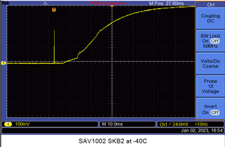
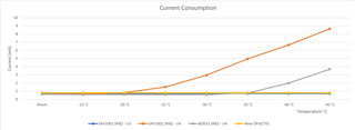
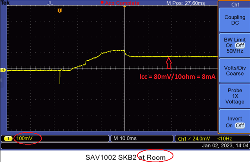
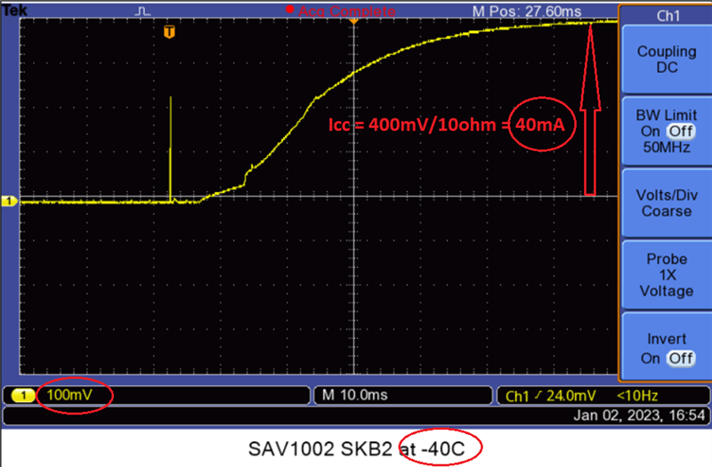
Recently we have encountered an issue with the current demand for one of four OPA2735AIDGKs in the circuit at -40 C. This is quite random and not found in all the PCBs and this can be any one of four while the fault exists. Following plots are the room temperature Vs -40 C current demand measured across a 10 ohm resistor , hence,  current = voltage/10. 
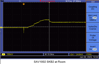
Any reason for this?

  • Hi Kavindu,

    what do you mean by "current demand"? The supply current of OPAmp? Where comes the ramp in the scope plots from? Is a power-up shown?

    Abnormal increase of supply current can have multiple causes. Can you show a complete schematic?

    Kai

  • As Kai said, we need to see your schematic including power supply voltage, input/output voltage and load.  Having said that, if this occurs during power-up, you need to keep in mind that below the minimum supply of 2.7V (or +/-1.35V) OPA2735 cannot bias up properly, which may result in much higher supply current.

  • Hi Kai,

    Thanks for the response. Yes, you are right that we are having issues with the supply current. And the plots are taken at power up instance. But later on we could observe that this issue is prevalent even during the steady state after power up. The schematics are attached - one is showing the amplification section while other is showing the power supply. Please note U1 and U2 are sourced by two different rails.PITCH CH.pdfPower and filtering.pdf

    Further, please find the attached on the steady-state current vs temperature of 4 OPA2735 s. You can observe the increase of current in 2 OPA2735s.

  • Hi Marek,

    Thank you for the response. Please find the information shared with Kai and hope it'd be helpful.

    Kavindu

  • Hi Kavindu,

    I cannot find U4 in the pdfs. Which OPAmp are we talking about?

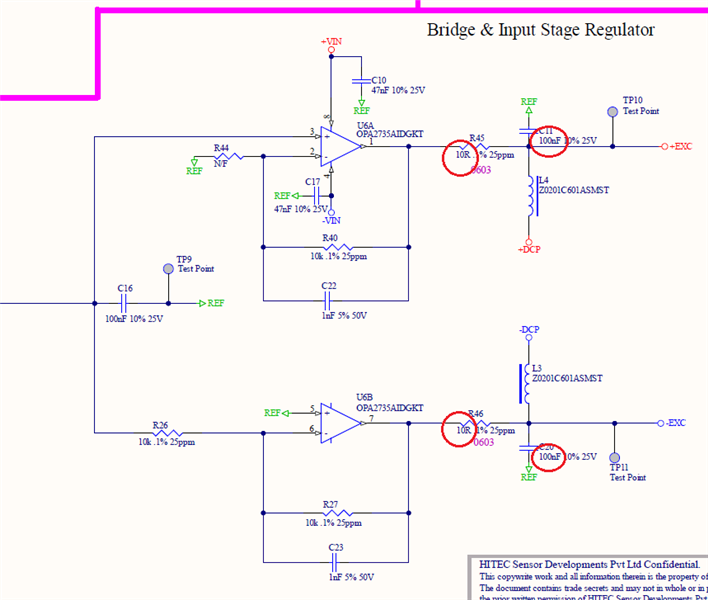
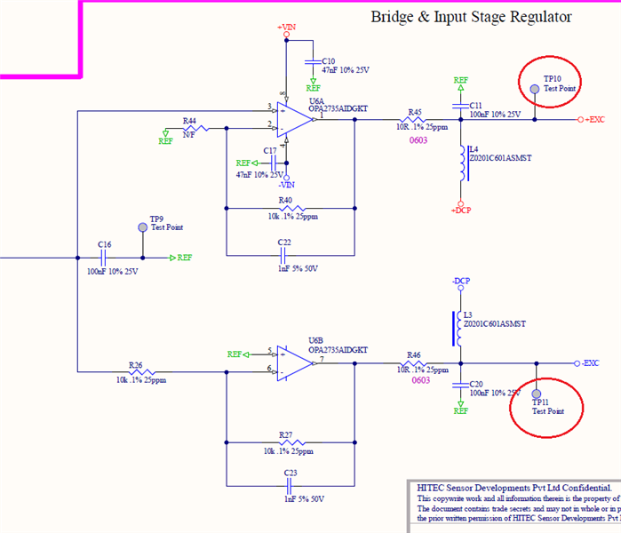
    Hhm, L3 and L4 look suspicious. Sharply turning-off the current through an inductance can produce an unwanted inductive kickback which can easily destroy the output of U6A or U6B. Diode clamps to the supply voltage rails of OPAmp may have to be added.

    Can you remove the L3 and L4 for a test? Also replace the OPAmps by fresh ones and check the supply currents again.

    Kai

  • Kavindu,

    I see U1, U2 and U6 on your schematics but as Kai mentioned no U4 that you show to draw higher current - please explain.  Also, all your circuits have load connected to their output so any change in Vout will cause change in the total current - where do you measure the current? As I said before, we need to see your schematic including power supply voltage, input/output voltage and load.

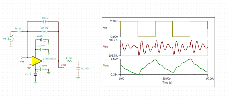
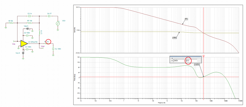
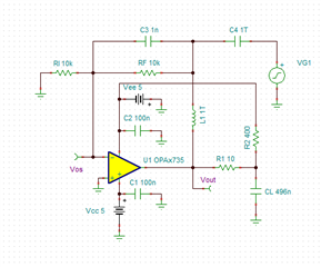
    Having said that the increased current may be related to the output oscillating - OPA735 cannot drive 100nF load with just 10 ohm series output resistor (R45).

    If you run transient analysis, you'll see a large overshoot - see below.

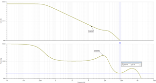
    AC simulation show a phase margin of just 8 degrees - see below - whereas the minimum recommended is 45 degrees.

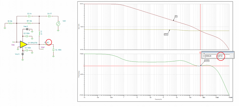
    In order to assure stable operation of the circuit you need to increase the R1 to at least 45ohms - see below.

    OPA735 Transient.TSC

    OPA735 AC stability.TSC

  • HI Kai,

    Thanks and apologies that I could not share the schematic of the other identical channel which is containing U4.Please find the attached.ROLL CH.pdf

    L3,L4 are ferrite beads to isolate the rails from the potential switching currents from digi pots and hope 10 ohm and 100 nF will snub any voltage kick back in case. But thank you for the suggestion. Here I should mention the current Vs Temperature plot has been generated with all 4 opams mounted on a vero board and applying power (+5V , -5V) separately hence tested in isolation. 

    And as you suggest we did replaced the fresh ones to see the issues vanished. So it helps for sure but we are trying to understand the root cause of the issue.

    Kavindu

  • Hi Marek,

    Thanks, I will come back to you on the stability topic, because I need a little recap.

    On the current draw issue, please find the missing bit of the schematic that I've attached in the response to Kai. In addition please see below details that you have requested.

     *.power supply voltage - This is a dual supply circuit +5V for P21 , 0V for P22, -5V for P23 (Please refer Power & Filtering section)

     *.Input - 5k wheaston bridge (Please refer Pitch/Roll input section)

    *.Output - Bipolar output +/- 4V

    *. Load - ~270 kOhm 

    As shared with Kai, please note that  the current Vs Temperature plot has been generated with all 4 opamps mounted on a vero board and applying power (+5V , -5V) separately, hence tested in isolation.

    Kavindu

  • Hi Kavindu,

    Since U1 and U2 are sourced by two different rails, which rail draw excessive current?  Have you replaced the parts with fresh ones, as Kai recommended, to eliminate the possibility of them being damaged due to inductive kickback?  Also, I believe a very likely cause of the increased current is instability of U6 outputs, resulting in the output charging/discharging 100nF loads - have you confirmed whether TP10 and TP11 show oscillation?

    In order to determine the actual cause behind increased supply current, first we need to start eliminating potential issues as outlined above. 

  • Hi Marek,

    Thank you for picking up again.

    Yes I agree that we need to look for all possibilities and rule out one by one.

    In case, as responded to Kai previously we could eliminate the issue by replacing the IC that was found to be drawing higher current with a fresh one.

    On the rail oscillation scenario that you suggested, we did a test run at room temperature and at -40C today while monitoring +/-Vin rail and +/-Exe rail and I can confirm that we could not observe any oscillation. Here we have captured oscilloscope graphs and we can share them if you need.  

    Appreciate further inputs from your end.

  • Hi Kavindu,

    hmm, the output of U6A would see through L4 all the decoupling caps hanging on +DCP. And not to forget the decoupling caps hanging on the +EXC line too. So, the capacitive load of U6A would be way higher than just C11??

    Kai

  • Kavindu,

    Since you confirmed that the increased current gets eliminated by replacing the IC with a fresh units, this means that you damage the part most likely due to inductive kickback.  For this reason you must add properly rated external Schottky diodes between the output and the rails - please review app note below:

    https://www.ti.com/lit/an/sboa447/sboa447.pdf?ts=1616630049631&ref_url=https%253A%252F%252Fwww.google.com%252F

    Having said that, I am not clear whether you think the above issue is separate from the increase current at cold temperature you showed at the top of this post. Analyzing the pics it is clear that the 8mA currents shown is way above the quiescent current even at room temperature (max specified 1.5mA for two channels), let alone 40mA at -40C, and thus either the increase in the current is due to heavier load or the output stage has been damaged (most likely by inductive kickback).

    As far as possible oscillation goes, it is completely unacceptable to go into production with typical 8 degrees phase margin (min 45 degrees is recommended).  This is because even though typical units will not have sustained oscillation,  wafer fab process variation will cause another batch of faster units to show unstable output.

  • Hi Marek,

    Thank you for the response.

    I need to clarify that the current measurement was done on the complete PCB that I shared the schematics on previous posts. And as we traced to the origin of the increased current the culprit was one of the opamps. 

    The kick back theory can be ruled out since U4 was also found to be defective, which has no relation to +/- EXC rails. Same with output instability theory. On the other hand if the output stages were blown due to some reason I doubt their proper functionality back at the room temperature which is perfectly ok on the defective units found so far.

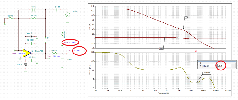
    Further I did another look at the phase margin and found that you have missed some information. So I revised the output capacitance to be   496nF to represent the worse case scenario and added a 400 ohm load between output and -EXC to represent the actual case. With those we are having a phase margin of 28 deg which I believe to be ok yet not ideal. That's why I think we are not seeing any oscillation in the real test curves.

    At this point can I suggest that if this can be a manufacturing defect related to a lot or a number of lots. Or is it too early for such an assumption provided Ti produces the best :) 

  • Hi Kavindu,

    I don't want to answer for Marek, but in my understanding a phase margin of 28° would be way too low. The minimum phase margin in OPAmp circuits is said to be 45°, while I choose a minimum phase margin of 60° in all of my circuits.

    Kai

  • Kavindu,

    Your modified circuit actually has only 25 degrees phase margin (see below) and as Kai pointed out the minimum recommended is 45 degrees.  This is because the simulation uses a typical model that does not include wafer fab process variation that may cause the GBW increasing by up to 30% resulting in the phase margin going down to zero.  Thus, you should NOT go to production with just 25 degrees phase margin if six months later you don't want to see output of the different OPA735 wafer lot to oscillate.

    Having said that, the R2 pulldown resistor results in the OPA735 sourcing 12.2mA current that due to voltage drop across 10ohm R1 will result in the VF1 error of -122mV ( see below).

    As far as the manufacturing defect goes, this is very unlikely on 20 year old part like OPA735 with no history of such defects.  Also, there are other possible reasons for such damage like power supply overshoot (I do not see TVS's on supply pins) that could simultaneously damage multiple op amps.

  • Hi Marek & Kai,

    I could find the root cause for this issue once I tested 200 chips from the reel before using them in the circuit. I put them under -40 C with separately wired only +Vcc and -Vcc and applied +/- 5 VDC and +/- 2.5 VDC in turn. There I could find few (3 to be exact) chips were drawing higher current than specified. At +/-5 VDC they tend to show a current draw of 4 mA and more interestingly as I dropped the supply voltage to +/- 2.5 VDC the currents increased to 10 mA! However the good parts were showing consistent current draw of ~ 0.8 mA regardless of the supply voltage. 

    Anyway thank you very much for your heads up on pointing out the possible causes of failure and the scope for improvements. 

  • Hi Kavindu,

    checking the issue with an extremely simplified test circuit is really a good idea! Bravo Relaxed

    But I have one question: Have you wired the OPAmps in any way to allow them to operate in their linear operation mode? If not, then I would connect the OPAmps as voltage follower (-input of OPAmp to output of OPAmp) and would connect the +input of OPAmp to signal ground. Otherwise the unconnected and floating inputs may cause additional issues.

    Kai

  • Kavindu,

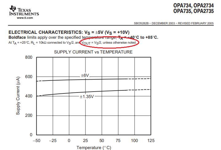
    Most of the analog IC's are designed for IQ with positive TC (increasing IQ with temperature) in order to keep the GBW constant - see below - but the change should not be more than 30% (PTAT).  

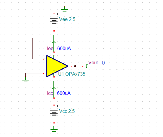
    Therefore, the tremendous variation in IQ you see must be caused by something else like damage to the part or floating input/output pins.  As Kai alluded to it, for any op amp to work properly you must use a negative feedback and bias the input at the ground (Vout=Vs/2 - mid-supply) to make sure that the input and output voltages are within the part's linear range (e.g. mid-supply in dual supply is ground).- see below: