This thread has been locked.

If you have a related question, please click the "Ask a related question" button in the top right corner. The newly created question will be automatically linked to this question.

OPA445: slew rate

Part Number: OPA445
Other Parts Discussed in Thread: OPA455, OPA462, OPA452

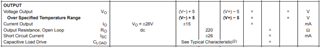
How can the OPA445 improve the slew rate of the noninverting and inverting amplifier circuits?

Currently, I am looking at the operation of the actual device, but the slew rate is several times smaller than the results of the simulation (slower)
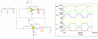
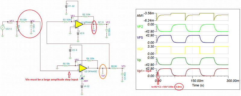
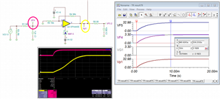
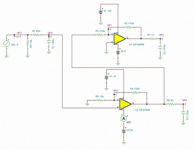
・diagram

・wave form

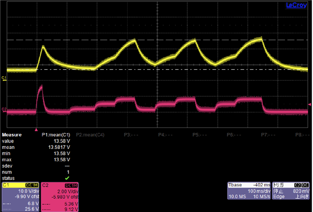
red: input(VF4), yellow: output(VF5)

Regards,

Hironori Kishida

Evident Corporation

opa445_amp.TSC

  • Hi Hironori-san,

    What was the load during the OPA445's tests in the scope capture?  I suspected that the output has reached the saturation based on the output swing specification. 

    Regarding to the slew rate, OPA445 has approx. 15V/usec. So from 0-45Vdc step, its rising and falling edges should be measured at approx. 45V/15V/usec ≈ 3 usec.  If this does not meet your design requirements, then you have to pick a different OPA400 series op amps with higher slew rate, such as OPA452, OPA455 or even OPA462. 

    In addition, please measure the op amp responses at Vp and Vp1 nodes under a load, since VF2 and VF5 nodes are measured after the LPFs with much larger RC time constant.  

    Please let us know your design requirements and may be we are able to provide you with additional suggestions. 

    Best,

    Raymond

  • In order for the op amp to slew, the input signal directly at the input terminal, Vin, must be a large amplitude (>1V) step signal.  Since Vin=VF4=-Vp is controlled by the low-pass time constant of R1*C1=5.6ms, the output simply follows the input since the input is too slow for the op amp to slew - see below. 

    In short, in order for the OPA445 to slew you must remove R1||C1 input filter.

  • Hi Marek, 

    Thanks for the comments! I overlooked the issue at the input.

    Best,

    Raymond 

  • Dear Raymond, Marek

    Thank you for your answer.

    The load is only 0.35uF capacitance.

    The following is the waveform of the actual board.

    pi22_Vin_TL2.tif

    red: input(VF4), yellow: output(Vp1)(20ms/div)


    The input signal rises from 0 V to 3.3 V in about 10 ms according to the time constant, while the output signal (yellow) rises by about 80 ms.

      * The input  is the waveform after passing through the RC filter, and the output  is the waveform before passing through the RC filter.

    Is the rise time much longer than the simulation results, but is it reasonable?

  • Hi Hironori-san,

    Is the rise time much longer than the simulation results, but is it reasonable?

    You should get similar output responses from the simulation. 

    From the screen shot, the output at Vp1 is measured at 32.3V and input at V4 is approx. 3.3V  --> the DUT's gain is approx. 32.3V/3.3V = 9.79 V/V

    If R5 = 10kΩ, R4 should be approx. 90kΩ, see the attached simulation. 

    opa445_amp 01112023.TSC

    I am unable to explain why Vp1 node has a significant longer response than the input at VF4.

    BTW, the OPA445's supply rails of 52Vdc and -6Vdc are used in the simulation. Please make sure that the power sources are not current limited in the bench setup. Perhaps you can send us a picture of the setup.

    Best,

    Raymond   

  • Hi Hironori,

    there's an issue with your supply voltages: It's always a bit dangerous to apply a signal to the input of an OPAmp which can exceed the supply voltages. U2 is powered by +52V but U1 only by +6V. If the supply voltages rise unevenly during the power-up, then the input voltage of U1 (coming from the output of U2) may heavily exceed its supply voltage. It's true that R3 limits the input current. But the OPA455 is from 1987 and there's a certain risk that the OPA445 responds this violation of absolute maximum ratings at the input with a latch-up or lock-up. Remember, the input voltage must stay 3V away from supply voltages. So, in my eyes there's a certain risk that the OPA455 is already damaged and that you see the performance of a damaged OPAmp.

    I would add a protection circuit to the -input of U1. I would give antiparallel clamping diodes from the -input to signal ground as shown in figure 16 of datasheet a try.

    The best remedy would be to power U1 and U2 with identical supply voltages, though.

    Kai

  • Hironori-san,

    Hi Kai, Thanks for the comments!

    Kai has good points. It did cross my mind that OPA455 may have damaged somewhere. Based on the bench tests, you may have unknowingly damaged the part, which the following absolute max. ratings may have exceed at some point.  

    If you have additional questions, please let us know. 

    Best,

    Raymond

  • Dear Raymond, Thanks for your answer.


    Is the input voltage range of U2 in this circuit

    Upper limit: +52V-3V=+49V , lower limit: -6V-3V=-9V?

    Regards,

  • Staying 3V away from the supply rails would mean +52V - 3V = +49V and -6V + 3V = -3V.

    Kai

  • Hi Kishida-san,

    Raymond is out for a few days.  Let me clarify, here, we are speaking about the OPA445, correct, and not OPA455?  Actually, the spec. that Raymond highlighted (abs. max.) is for voltages that can cause device failure, but important to keep in mind that for proper functionality, the device actually needs to be configured with a common-mode input voltage that is 5 V from the rail.  This can be seen in the common mode input spec:

    Otherwise, it appears the bandwidth is limited by the input filter, as Marek had mentioned.

    Let us know any other questions.

    Regards,
    Mike