This thread has been locked.

If you have a related question, please click the "Ask a related question" button in the top right corner. The newly created question will be automatically linked to this question.

INA190: Read 4-20mA current with INA190 + ADC Microcontroller

Part Number: INA190
Other Parts Discussed in Thread: INA185, INA191, INA180, INA293, INA281, INA199, OPA320, OPA325

Hello dears,

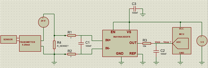
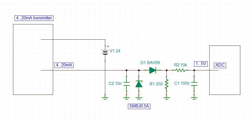
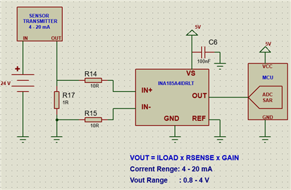
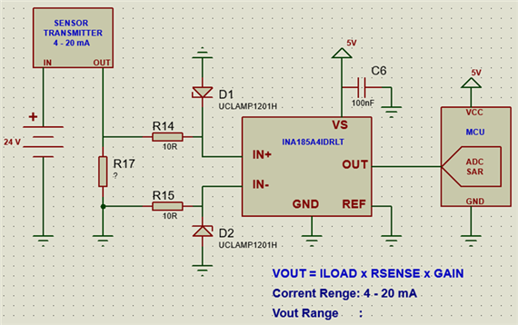
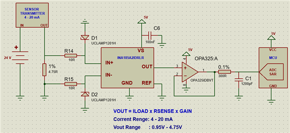
We are trying to develop a receiver that allows reading 4 – 20mA current from industrial transmitters and converting it to voltage to be processed by the ADC of a Microcontroller. I am attaching the schematic diagram, I need to know if it is correct or if you could recommend any parts for our application.

I appreciate your help.

  • Hi Ivan,

    looks a bit like overengineering with the INA190. Also, the wiring of 2-wire transmitter looks a bit weird.

    I would do it this way:

    C2 and the TVS form a EMI filter and protection circuit against ESD, Surge and Burst. Only a low leakage TVS must be just here, for instance from ST. Eventually a SMBJ8.5A may also be used. D1 is a protection against negative input voltages and reverse currents. R1 transforms the 4..20mA input current into a voltage of 1..5V. And R2 and C1 form a charge kickback filter for the ADC and serve as input low pass filter (anti-aliasing filter). R2 in combination with the internal protection diodes of ADC to the supply rails also protects the ADC against overvoltages by limiting the input current. If the ADC has no internal input protection diodes, add external ones from C1 to the supply rails.

    Three more points:

    1. R2 = 10k is a bit high and can make issues, if the ADC  has high input leakage currents. Then R2 should be decreased.

    2. The supply voltage must be able to absorb the reverse current during an overvoltage event. Eventually a suited TVS from the supply voltage to signal ground has to be added to absorb the reverse current and to limit the supply voltage.

    3. If the ADC has a different input voltage range, R1 must be modified accordingly.

    Kai

  • Hello Ivan,

    I am looking this over and will respond shortly.

    Best,

    Peter

  • Hello Peter,
    Thank you very much, I will be attentive.

    Greetings.

  • Hey Ivan,

    So this is a perfectly valid circuit to measure the 4-20mA signal. I will say the charge bucket filter (R3 and C2) are not optimal for many SAR converters operating with short conversion and acquisition times. But at the end what matters is what your system requirements are such as maximum error at low current, required signal BW, IQ limit, and required source impedance to accurately drive the ADC.

    The INA190 is nice because it is low power, low offset, and low IB (nA). The low IB (high input impedance) means that input bias current won't subtract from the 4mA signal and create error. It also means you can put a heft input filter (R1=R2=1kΩs) and attenuate a line noise. However, many of our current sense amplifiers (CSAs) will have single µA IB at low side (Vcm=0V), so having the low IB may not be critical. An example would be the INA185, which has -6µA IB at Vcm=0V.

    The INA185 also has much better BW so it may be able to drive the ADC better.

    The other consideration is if you have to measure a signal that can start at 0A. If REF=GND and load starts at 0mA, then Vout will be starting in saturation and there will be required settling time for a step response, but this may not be important because you won't start recording data until signal is at 4mA. If this is the case, then you can pick a device that does not have a REF pin such as the INA191, INA180, INA293.

    The INA293/INA281 is nice because it has good BW and accuracy, so it could easily drive many SAR ADCs even at fast acquisition rates. The drawback is increase IQ.

    The INA185 is nice because it has small package, decent BW, and accuracy so it could potentially drive the ADC by itself. It is also specified at Vcm=0V, which can help narrow the error range.

    Keep in mind that all of the models I have mentioned have simulaiton models that include closed-loop output impedance (Zout), which is very useful when optimizing the R3 and C2 anti-aliasing filter for a specific ADC operating at a specific speed. Here is an application describing the process.

    CSA Considerations for Driving SAR ADCs

    As for determining max possible error, this can be approached theoretically using standard amplifier RSS error equations found in our training material.

    https://www.ti.com/video/series/ti-precision-labs-current-sense-amplifiers.html

    https://www.ti.com/video/series/ti-precision-labs-current-sense-amplifiers.html

    Low (microamp), high-side, current-sensing circuit with current-sensing amp

    Sincerely,

    Peter

  • Hello Peter,

    Thanks for the reply, I have changed the INA190 to the INA185 as you suggested.
    I have the following queries:
    1) Are the 10R resistors necessary at the input?
    2) Do you recommend placing a filter on the INA185 OUT pin?
    3) According to the attached image, is the connection of the 4-20mA transmitter correct?

  • Hi Ivan,

    if the INA185 is remote and cabling is involved, you may need protection against ESD, Surge, Burst, EMI and reverse voltages at the input of INA185, as discussed in my post above. Keep in mind that the INA185 becomes damaged, when the input voltage goes more negative than -0.3V.

    Whether you need a charge bucket filter at the input of ADC of µC mainly depends on this ADC itself. The datasheet of ADC usually recommends a suited charge bucket filter. Keep in mind, though, that the output of INA185 in combination with the charge bucklet filter must fully settle within the aquisition time of ADC. Unfortunately, the settling time of INA185 is not specified in the datasheet. But from figure 27 you can see that it needs several µs to fully settle. So, it may be necessary to program a sufficiently long aquisition time for the ADC in the µC. If this is not possible, you may need an additional ADC driver which is fast enough to be able to fully settle within the aquisition time of ADC.

    What µC are using and what aquisition time is programmed?

    Why are you using a so small burden resistor? 1R is very unsual. Or do you plan to have more than one burden resistor in series? And if so, are you sure that you can reference your burden resistor to signal ground?

    Kai

  • Hello Kai,
    Thank you very much for the answer, then I answer your questions.

    1) The microcontroller used is AVR32DA28, I attach configuration images:

    uC Configuration:

    2) A single load resistor will be used, what load resistor do you recommend to use to get an output voltage (0.5V >= Vout <= 4V) ?

    Thanks for your help.

    Ivan

  • Hello Ivan,

    Kai is correct that you need to consider any long cables/traces involved here with the input pins or output pin of the INA185. Long transmission lines mean inductance and this voltage changes can cause inductive kickback and potentially pull pin voltages below -0.3V. 

    Thus, 10-Ohm input resistors can help limit inductive kickback current, but system validation would be needed to know if it is enough. This is where the INA199 would be advantageous as you could replace the with 1kOhm resistors. Although you would need a differential capacitor between IN- and IN+ pins to stabilize this. See section applications section of datasheet.

    The other reason to keep the input resistors would be to create a differential input pin filter to filter current noise. Once again this requires system testing and validation to see if this is necessary.

    You should probably at least include pads for a RC filter at OUT pin of INA185 / input of ADC. Charge buckets are usually needed to maintain ADC accuracy. This application should provide some insight:

    https://www.ti.com/lit/an/sboa443/sboa443.pdf?ts=1649717236896&ref_url=https%253A%252F%252Fwww.google.com%252F

    Sincerely,

    Peter

  • Hello Ivan,

    In the application note I sent, it goes through the equations you can use to approximate a first-pass Rfilt and Cfilt for ADC input pin. Based upon the ADC setting you have sent I tried to calculate what the acquisition time will be and plug this into the calculator this application note is based around. The calculator is called the Analog Engineer's Calculator.

    Here are the first pass results.

    Unfortunately, the processor datasheet does not detail what the typical input capacitance is for the ADC (Csh), so maybe contact maufacturer to see if they can give you a value. Also, know that the MUX is going to add some capacitance to the Cfilt value, so the Cfilt you use may actually need to be the Cfilt calculated minus the Cmux. If you can get these capacitances, you can go through with a SPICE simulation procedure (outlined in the aforementioned application note) to determine the optimal Rfilt and Cfilt such that the ADC voltage falls to under 0.5LSB.

    The other way to fine tune the Rfilt and Cfilt is through actual system testing. You could measure the ADC input voltage with accurate volt-meter and compare to ADC readings. You could also make the board with a operational amplifier buffer (e.g., OPA320) in between the current-sense amplifier (CSA) (i.e., INA185) and test if there is any significant degradation of accuracy when ADC has the buffer and when it does not.

    Even if you do use a buffer, you will still want the have pads for this Rfilt, Cfilt as you may end up needing them anyway as it is usual best practice.

    As for setting the Rsh. You need to understand what is the maximum shunt voltage drop allowed and/or what is the maximum shunt power dissipation allowed in your system, this will set the upper bounds of Rsh. Then to get the best error, set the Rsh to highest possible value based upon max current and CSA gain and CSA max Vout. I usually choose max Vout to be 4.85V (note consult Figure 19 to see if Vout could go lower if Iout can exceed 1.5mA. Also note that Iout can peak for high value of Cfilt, another reason to use simulation to determine this transient Iout).

    So if Vout_max is 4.85V, then Vin_max for INA185A2 (50V/V) is 4.85/50 = 97mV. Thus Rsh_typical = 97mV/20mA = 4.85-Ω. Round this down to nearest available resistor.

    Sincerely,

    Peter

  • Hello Peter,

    Thanks for the detailed explanation.

    So I have modified the circuit, I will also replace the OPA320 with an OPA325 since my supplier does not have stock.

    Ivan.