Other Parts Discussed in Thread: INA225, CSD
Hello Team
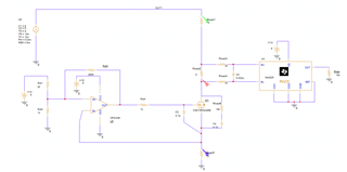
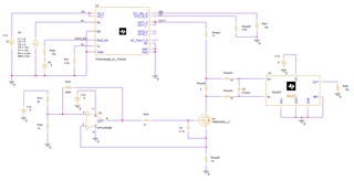
We are trying to simulate the spice circuit on PSpice & LtSpice but we are getting some error with library of TPS2H000B
In case of pspice, I have used same simulation profile that is available on TI's website in design support section.
And in case of LtSpice using Library file provided by TI.
Attaching the schematic and output file from both Pspice and LtSpice
We have grounded the SEL pin. Is it correct?
Your support will be much appreciated.
Regards,
Sandip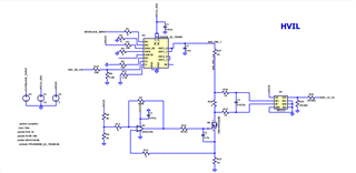
INA225_AC_TRANS.txt
**** 04/21/23 17:29:03 **** PSpice 17.4.0 (4 January 2023) **** ID# 0 ********

 ** Profile: "INA225_TRANS_AC-INA225_AC_TRANS"  [ C:\Users\sm925214.ttl\OneDrive - TATA MOTORS LTD\LTspice\Libraries\HVIL\INA225_PSPI


 ****     CIRCUIT DESCRIPTION


******************************************************************************


** Creating circuit file "INA225_AC_TRANS.cir"
** WARNING: THIS AUTOMATICALLY GENERATED FILE MAY BE OVERWRITTEN BY SUBSEQUENT SIMULATIONS

*Libraries:
* Profile Libraries :
* Local Libraries :
.LIB "../../../ina225.lib"
* From [PSPICE NETLIST] section of C:\Users\sm925214.ttl\cdssetup\OrCAD_PSpice\17.4.0\PSpice.ini file:
.lib "nom.lib"

*Analysis directives:
.TRAN  0 4ms 0 1u
.OPTIONS ADVCONV
.PROBE64 V(alias(*)) I(alias(*))
.INC "..\INA225_TRANS_AC.net"


**** INCLUDING INA225_TRANS_AC.net ****
* source INA225
R_R1         VMID VOUT  10k TC=0,0
E_E1         VMID 0 VCC 0 0.5
V_V1         VCC 0 5Vdc
V_VCM         VIN+ 0 12Vdc
C_C1         VOUT VMID  10p  TC=0,0
V_V2         VIN+ VIN- DC 0 AC 1 Sin(0 10m 1KHz)
V_V3         N241886 0 5Vdc
V_V4         N241892 0 5Vdc
X_U1         VIN+ VIN- VCC 0 VMID N241892 N241886 VOUT INA225
V_V6         IN 0
+PULSE 0 5 0 10n 10n 0.8m 5m
X_U3         N14948818 N14948795 N14948795 DIAG_EN VS VS IN 0 CL CS 0 SEL 0
+  OUT1 OUT1 0 0 TPS2H000B_Q1_TRANS
V_V8         N14941166 0 5
R_Rload1         OUT1 N14939328  1k TC=0,0
R_Rcl         CL 0  3.2k TC=0,0
X_U4         N14943376 N14943390 N14943758 0 0 0 0 N14944503 INA225
X_M1         N14943217 N14946461 N14945020 IPB05N03L_L1 PARAMS:
X_U5         N14945411 N14945020 N14945955 0 N14946017 OPA336/BB
R_Rcs1         SEL 0  10k TC=0,0
R_Rcs2         DIAG_EN N14941166  10k TC=0,0
R_Rload2         N14939328 N14943217  2 TC=0,0
R_Rload3         N14939328 N14943376  10 TC=0,0
R_Rload4         N14943217 N14943390  10 TC=0,0
C_C2         N14943376 N14943390  0.022u  TC=0,0
V_V12         VS 0 12
V_V13         N14943758 0 5
R_Rcs3         N14944503 0  10k TC=0,0
R_Rload5         0 N14945020  10 TC=0,0
V_V14         N14945399 0 5
R_Rcl1         N14945399 N14945411  2k TC=0,0
R_Rcl2         N14945411 0  1k TC=0,0
V_V15         N14945955 0 5
R_Rcl3         N14945411 N14946017  200k TC=0,0
R_Rcl4         N14946017 N14946461  1k TC=0,0
C_C3         N14946461 N14945020  4.7p  TC=0,0
R_Rload6         CS 0  4.8k TC=0,0

**** RESUMING INA225_AC_TRANS.cir ****
.END


ERROR(ORPSIM-15108): Subcircuit TPS2H000B_Q1_TRANS used by X_U3 is undefined


**** EXPANSION OF SUBCIRCUIT X_U1.X_U16 ****
.PARAM VTHR 1
.PARAM GL 1e3
.PARAM RMAX 1e6
.PARAM GET1 3e-6
.PARAM GET2 5e-6
X_U1.X_U16.EGET1 X_U1.X_U16.NGET1 0 VALUE {1 + GET1*(TEMP-27)}
X_U1.X_U16.EGET2 X_U1.X_U16.NGET2 0 VALUE {1 + GET2*(TEMP-27)}
X_U1.X_U16.ES0 X_U1.X_U16.NS0 0 VALUE {MAX(MIN(GL*(V(1#)-VTHR),1),0)}
X_U1.X_U16.ES1 X_U1.X_U16.NS1 0 VALUE {MAX(MIN(GL*(V(0#)-VTHR),1),0)}
X_U1.X_U16.E00 X_U1.X_U16.N00 0 VALUE {(1-V(NS1))*(1-V(NS0))}
X_U1.X_U16.E01 X_U1.X_U16.N01 0 VALUE {(1-V(NS1))*(V(NS0))}
X_U1.X_U16.E10 X_U1.X_U16.N10 0 VALUE {(V(NS1))*(1-V(NS0))}
X_U1.X_U16.E11 X_U1.X_U16.N11 0 VALUE {(V(NS1))*(V(NS0))}
X_U1.X_U16.ESW X_U1.X_U16.NSW 0 VALUE {V(NGET1)*(8*V(N00) + 4*V(N01) +
+ 2*V(N10))+ V(NGET2)*V(N11)}
X_U1.X_U16.G1 VOUT X_U1.INN VALUE {V(NSW)*(V(3#,2#)/RMAX)} }
-----------------------------------------------------------$
ERROR(ORPSIM-16318): Missing or invalid expression


**** EXPANSION OF SUBCIRCUIT X_U1.X_U15 ****
.PARAM VTHR 1
.PARAM GL 1e3
.PARAM RMAX 1e6
.PARAM GET1 3e-6
.PARAM GET2 5e-6
X_U1.X_U15.EGET1 X_U1.X_U15.NGET1 0 VALUE {1 + GET1*(TEMP-27)}
X_U1.X_U15.EGET2 X_U1.X_U15.NGET2 0 VALUE {1 + GET2*(TEMP-27)}
X_U1.X_U15.ES0 X_U1.X_U15.NS0 0 VALUE {MAX(MIN(GL*(V(1#)-VTHR),1),0)}
X_U1.X_U15.ES1 X_U1.X_U15.NS1 0 VALUE {MAX(MIN(GL*(V(0#)-VTHR),1),0)}
X_U1.X_U15.E00 X_U1.X_U15.N00 0 VALUE {(1-V(NS1))*(1-V(NS0))}
X_U1.X_U15.E01 X_U1.X_U15.N01 0 VALUE {(1-V(NS1))*(V(NS0))}
X_U1.X_U15.E10 X_U1.X_U15.N10 0 VALUE {(V(NS1))*(1-V(NS0))}
X_U1.X_U15.E11 X_U1.X_U15.N11 0 VALUE {(V(NS1))*(V(NS0))}
X_U1.X_U15.ESW X_U1.X_U15.NSW 0 VALUE {V(NGET1)*(8*V(N00) + 4*V(N01) +
+ 2*V(N10))+ V(NGET2)*V(N11)}
X_U1.X_U15.G1 VMID X_U1.INP VALUE {V(NSW)*(V(3#,2#)/RMAX)} }
-----------------------------------------------------------$
ERROR(ORPSIM-16318): Missing or invalid expression


**** EXPANSION OF SUBCIRCUIT X_U4.X_U16 ****
.PARAM VTHR 1
.PARAM GL 1e3
.PARAM RMAX 1e6
.PARAM GET1 3e-6
.PARAM GET2 5e-6
X_U4.X_U16.EGET1 X_U4.X_U16.NGET1 0 VALUE {1 + GET1*(TEMP-27)}
X_U4.X_U16.EGET2 X_U4.X_U16.NGET2 0 VALUE {1 + GET2*(TEMP-27)}
X_U4.X_U16.ES0 X_U4.X_U16.NS0 0 VALUE {MAX(MIN(GL*(V(1#)-VTHR),1),0)}
X_U4.X_U16.ES1 X_U4.X_U16.NS1 0 VALUE {MAX(MIN(GL*(V(0#)-VTHR),1),0)}
X_U4.X_U16.E00 X_U4.X_U16.N00 0 VALUE {(1-V(NS1))*(1-V(NS0))}
X_U4.X_U16.E01 X_U4.X_U16.N01 0 VALUE {(1-V(NS1))*(V(NS0))}
X_U4.X_U16.E10 X_U4.X_U16.N10 0 VALUE {(V(NS1))*(1-V(NS0))}
X_U4.X_U16.E11 X_U4.X_U16.N11 0 VALUE {(V(NS1))*(V(NS0))}
X_U4.X_U16.ESW X_U4.X_U16.NSW 0 VALUE {V(NGET1)*(8*V(N00) + 4*V(N01) +
+ 2*V(N10))+ V(NGET2)*V(N11)}
X_U4.X_U16.G1 N14944503 X_U4.INN VALUE {V(NSW)*(V(3#,2#)/RMAX)} }
----------------------------------------------------------------$
ERROR(ORPSIM-16318): Missing or invalid expression


**** EXPANSION OF SUBCIRCUIT X_U4.X_U15 ****
.PARAM VTHR 1
.PARAM GL 1e3
.PARAM RMAX 1e6
.PARAM GET1 3e-6
.PARAM GET2 5e-6
X_U4.X_U15.EGET1 X_U4.X_U15.NGET1 0 VALUE {1 + GET1*(TEMP-27)}
X_U4.X_U15.EGET2 X_U4.X_U15.NGET2 0 VALUE {1 + GET2*(TEMP-27)}
X_U4.X_U15.ES0 X_U4.X_U15.NS0 0 VALUE {MAX(MIN(GL*(V(1#)-VTHR),1),0)}
X_U4.X_U15.ES1 X_U4.X_U15.NS1 0 VALUE {MAX(MIN(GL*(V(0#)-VTHR),1),0)}
X_U4.X_U15.E00 X_U4.X_U15.N00 0 VALUE {(1-V(NS1))*(1-V(NS0))}
X_U4.X_U15.E01 X_U4.X_U15.N01 0 VALUE {(1-V(NS1))*(V(NS0))}
X_U4.X_U15.E10 X_U4.X_U15.N10 0 VALUE {(V(NS1))*(1-V(NS0))}
X_U4.X_U15.E11 X_U4.X_U15.N11 0 VALUE {(V(NS1))*(V(NS0))}
X_U4.X_U15.ESW X_U4.X_U15.NSW 0 VALUE {V(NGET1)*(8*V(N00) + 4*V(N01) +
+ 2*V(N10))+ V(NGET2)*V(N11)}
X_U4.X_U15.G1 0 X_U4.INP VALUE {V(NSW)*(V(3#,2#)/RMAX)} }
--------------------------------------------------------$
ERROR(ORPSIM-16318): Missing or invalid expression
error log.txt
Circuit: * C:\Users\sm925214.ttl\OneDrive - TATA MOTORS LTD\LTspice\VCU Sandip Sir\HVIL\Design 1\Design 1.asc

Questionable use of curly braces in "b§e_abmgate yint 0 v={if(v(a)>{{vthresh}}|v(b)>{{vthresh}},{{vdd}},{{vss}})}"
    Error: undefined symbol in: "if([v](a)>((vthresh))|v(b)>((vthresh)),((vdd)),((vss)))"
Questionable use of curly braces in "b§e_abmgate yint 0 v={if(v(a)>{{vthresh}}|v(b)>{{vthresh}},{{vdd}},{{vss}})}"
    Error: undefined symbol in: "if([v](a)>((vthresh))|v(b)>((vthresh)),((vdd)),((vss)))"
Questionable use of curly braces in "b§e_abmgate yint 0 v={if(v(a)>{{vthresh}},{{vss}},{{vdd}})}"
    Error: undefined symbol in: "if([v](a)>((vthresh)),((vss)),((vdd)))"
Questionable use of curly braces in "b§e_abmgate yint 0 v={if(v(a)>{{vthresh}}|v(b)>{{vthresh}},{{vdd}},{{vss}})}"
    Error: undefined symbol in: "if([v](a)>((vthresh))|v(b)>((vthresh)),((vdd)),((vss)))"
Questionable use of curly braces in "b§e_abmgate yint 0 v={if(v(a)>{{vthresh}}|v(b)>{{vthresh}}|v(c)>{{vthresh}},{{vdd}},{{vss}})}"
    Error: undefined symbol in: "if([v](a)>((vthresh))|v(b)>((vthresh))|v(c)>((vthresh)),((vdd)),((vss)))"
Questionable use of curly braces in "b§e_abmgate yint 0 v={if(v(a)>{{vthresh}},{{vss}},{{vdd}})}"
    Error: undefined symbol in: "if([v](a)>((vthresh)),((vss)),((vdd)))"
Questionable use of curly braces in "b§e_abmgate yint 0 v={if(v(a)>{{vthresh}},{{vss}},{{vdd}})}"
    Error: undefined symbol in: "if([v](a)>((vthresh)),((vss)),((vdd)))"
Questionable use of curly braces in "b§e_abmgate yint 0 v={if(v(a)>{{vthresh}},{{vss}},{{vdd}})}"
    Error: undefined symbol in: "if([v](a)>((vthresh)),((vss)),((vdd)))"
Questionable use of curly braces in "b§e_abmgate yint 0 v={if(v(a)>{{vthresh}},{{vss}},{{vdd}})}"
    Error: undefined symbol in: "if([v](a)>((vthresh)),((vss)),((vdd)))"
Questionable use of curly braces in "b§e_abmgate yint 0 v={if(v(a)>{{vthresh}}&v(b)>{{vthresh}},{{vdd}},{{vss}})}"
    Error: undefined symbol in: "if([v](a)>((vthresh))&v(b)>((vthresh)),((vdd)),((vss)))"
Questionable use of curly braces in "b§e_abmgate yint 0 v={if(v(a)>{{vthresh}},{{vss}},{{vdd}})}"
    Error: undefined symbol in: "if([v](a)>((vthresh)),((vss)),((vdd)))"
Questionable use of curly braces in "b§e_abmgate yint 0 v={if(v(a)>{{vthresh}},{{vss}},{{vdd}})}"
    Error: undefined symbol in: "if([v](a)>((vthresh)),((vss)),((vdd)))"
Questionable use of curly braces in "b§e_abmgate yint 0 v={if(v(a)>{{vthresh}}&v(b)>{{vthresh}},{{vdd}},{{vss}})}"
    Error: undefined symbol in: "if([v](a)>((vthresh))&v(b)>((vthresh)),((vdd)),((vss)))"
Questionable use of curly braces in "b§e_abmgate yint 0 v={if(v(a)>{{vthresh}}|v(b)>{{vthresh}}|v(c)>{{vthresh}},{{vdd}},{{vss}})}"
    Error: undefined symbol in: "if([v](a)>((vthresh))|v(b)>((vthresh))|v(c)>((vthresh)),((vdd)),((vss)))"
Questionable use of curly braces in "b§e_abmgate yint 0 v={if(v(a)>{{vthresh}},{{vss}},{{vdd}})}"
    Error: undefined symbol in: "if([v](a)>((vthresh)),((vss)),((vdd)))"
Questionable use of curly braces in "b§e_abmgate yint 0 v={if(v(a)>{{vthresh}},{{vss}},{{vdd}})}"
    Error: undefined symbol in: "if([v](a)>((vthresh)),((vss)),((vdd)))"
Questionable use of curly braces in "b§e_abmgate yint 0 v={if(v(a)>{{vthresh}},{{vss}},{{vdd}})}"
    Error: undefined symbol in: "if([v](a)>((vthresh)),((vss)),((vdd)))"
Questionable use of curly braces in "b§e_abmgate yint 0 v={if(v(a)>{{vthresh}}|v(b)>{{vthresh}},{{vdd}},{{vss}})}"
    Error: undefined symbol in: "if([v](a)>((vthresh))|v(b)>((vthresh)),((vdd)),((vss)))"
Questionable use of curly braces in "b§e_abmgate yint 0 v={if(v(a)>{{vthresh}}|v(b)>{{vthresh}},{{vdd}},{{vss}})}"
    Error: undefined symbol in: "if([v](a)>((vthresh))|v(b)>((vthresh)),((vdd)),((vss)))"
Questionable use of curly braces in "b§e_abmgate yint 0 v={if(v(a)>{{vthresh}}&v(b)>{{vthresh}},{{vdd}},{{vss}})}"
    Error: undefined symbol in: "if([v](a)>((vthresh))&v(b)>((vthresh)),((vdd)),((vss)))"
Questionable use of curly braces in "b§e_abmgate yint 0 v={if(v(a)>{{vthresh}},{{vss}},{{vdd}})}"
    Error: undefined symbol in: "if([v](a)>((vthresh)),((vss)),((vdd)))"
Questionable use of curly braces in "b§e_abmgate yint 0 v={if(v(a)>{{vthresh}},{{vss}},{{vdd}})}"
    Error: undefined symbol in: "if([v](a)>((vthresh)),((vss)),((vdd)))"
Questionable use of curly braces in "b§e_abmgate yint 0 v={if(v(a)>{{vthresh}},{{vdd}},{{vss}})}"
    Error: undefined symbol in: "if([v](a)>((vthresh)),((vdd)),((vss)))"
Questionable use of curly braces in "b§e_abmgate yint 0 v={if(v(a)>{{vthresh}},{{vdd}},{{vss}})}"
    Error: undefined symbol in: "if([v](a)>((vthresh)),((vdd)),((vss)))"
Warning: Multiple definitions of model "nmos01" Type: Mos1
WARNING: Less than two connections to node adc_hs_cs.  This node is used by r10.
WARNING: Less than two connections to node adc_ls_cs.  This node is used by r24.
WARNING: Less than two connections to node n010.  This node is used by r:u3:_r3.
WARNING: Less than two connections to node n005.  This node is used by s:u3:_s3:_s3.
Instance "m:u2:7": Length shorter than recommended for a level 1 MOSFET.
Instance "m:u2:3": Length shorter than recommended for a level 1 MOSFET.
Instance "m:u2:4": Length shorter than recommended for a level 1 MOSFET.
Instance "m:u2:8": Length shorter than recommended for a level 1 MOSFET.
Instance "m:u2:9": Length shorter than recommended for a level 1 MOSFET.
Instance "m:u2:9c": Length shorter than recommended for a level 1 MOSFET.
Instance "m:u2:1": Length shorter than recommended for a level 1 MOSFET.
Instance "m:u2:2": Length shorter than recommended for a level 1 MOSFET.
Instance "m:u2:113": Length shorter than recommended for a level 1 MOSFET.
Instance "m:u2:114": Length shorter than recommended for a level 1 MOSFET.
u3:_u1_u2_u21:dd: Emission coefficient, N=0.01, too small, limited to 0.1
u3:_u1_u2_u20:dd: Emission coefficient, N=0.01, too small, limited to 0.1
u3:_u1_u2_u22:dd: Emission coefficient, N=0.01, too small, limited to 0.1
u3:_u1_u2_u25:dd: Emission coefficient, N=0.01, too small, limited to 0.1
u3:_u1_u3_u21:dd: Emission coefficient, N=0.01, too small, limited to 0.1
u3:_u1_u3_u22:dd: Emission coefficient, N=0.01, too small, limited to 0.1
u3:_u1_u3_u20:dd: Emission coefficient, N=0.01, too small, limited to 0.1
u3:_u2_u3_u21:dd: Emission coefficient, N=0.01, too small, limited to 0.1
u3:_u2_u3_u22:dd: Emission coefficient, N=0.01, too small, limited to 0.1
u3:_u2_u3_u20:dd: Emission coefficient, N=0.01, too small, limited to 0.1
u3:_u2_u2_u22:dd: Emission coefficient, N=0.01, too small, limited to 0.1
u3:_u2_u2_u21:dd: Emission coefficient, N=0.01, too small, limited to 0.1
u3:_u2_u2_u25:dd: Emission coefficient, N=0.01, too small, limited to 0.1
u3:_u2_u2_u20:dd: Emission coefficient, N=0.01, too small, limited to 0.1
Direct Newton iteration for .op point skipped.
Starting Gmin stepping
Gmin = 10
Gmin = 1.07374
vernier = 0.5
vernier = 0.25
vernier = 0.125
Gmin = 0.439805
vernier = 0.0625
vernier = 0.03125
vernier = 0.015625
Gmin = 0.41504
vernier = 0.0078125
vernier = 0.00390625
vernier = 0.00195312
vernier = 0.000976562
Gmin = 0.414129
vernier = 0.000488281
Gmin = 0
Gmin stepping succeeded in finding the operating point.

Ignoring empty pin current: Ix(u3:out2_1)
Ignoring empty pin current: Ix(u3:vs_1)
Ignoring empty pin current: Ix(u3:out1_1)
Ignoring empty pin current: Ix(u3:out2_1)
Ignoring empty pin current: Ix(u3:vs_1)
Ignoring empty pin current: Ix(u3:out1_1)
Heightened Def Con from 0.00050139 to 0.000501409
Heightened Def Con from 0.00150139 to 0.00150141
Heightened Def Con from 0.00250139 to 0.00250141
Heightened Def Con from 0.00350139 to 0.00350139
Heightened Def Con from 0.00450151 to 0.00450151
Heightened Def Con from 0.00450151 to 0.00450151
Heightened Def Con from 0.00550148 +to 0.00550148
Heightened Def Con from 0.00627359 to 0.00627361
Heightened Def Con from 0.00650139 to 0.00650141
Heightened Def Con from 0.00750139 to 0.00750139
Heightened Def Con from 0.00927359 to 0.00927359
Heightened Def Con from 0.00927359 +to 0.00927359
Heightened Def Con from 0.00950139 to 0.00950139

Date: Fri Apr 21 17:45:02 2023
Total elapsed time: 5.702 seconds.

tnom = 27
temp = 27
method = modified trap
totiter = 47247
traniter = 45877
tranpoints = 14884
accept = 11862
rejected = 3037
matrix size = 735
fillins = 447
solver = Normal
Avg thread counts: 1.0/1.0/1.0/1.0
Matrix Compiler1: 43.52 KB object code size  27.8/19.5/[4.2]
Matrix Compiler2: off  [8.3]/13.1/12.0