This thread has been locked.

If you have a related question, please click the "Ask a related question" button in the top right corner. The newly created question will be automatically linked to this question.

OPA818: The actual bandwidth of the TIA circuit cannot meet the design requirements

Part Number: OPA818

During the debugging of OPA818, it was found that the bandwidth could not meet the design specifications, and it was suspected that it was the influence of parasitic capacitance, but I did not know how to eliminate it.

Design the circuit according to chapter 9.2 of the datasheet, the first version of PCB (thickness 1.0mm), Rf changed to 50kR, after the feedback capacitance is less than 0.3pF, change the feedback capacitor value, there is no significant impact on the bandwidth (bandwidth between 11MHz~14MHz, can not exceed 14MHz), remove the feedback capacitor network, the circuit still works normally, the bandwidth is 14MHz.

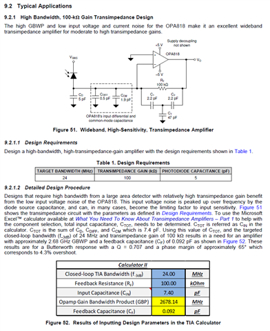
The first version of the PCB (thickness 1.0mm) changed the Rf from a single 50kR (0603 package) resistor to 20kR and 30kR resistors in series (0603 footprint), without feedback capacitors, and the bandwidth can be increased to 19MHz. However, it is still below the indicators in the manual.

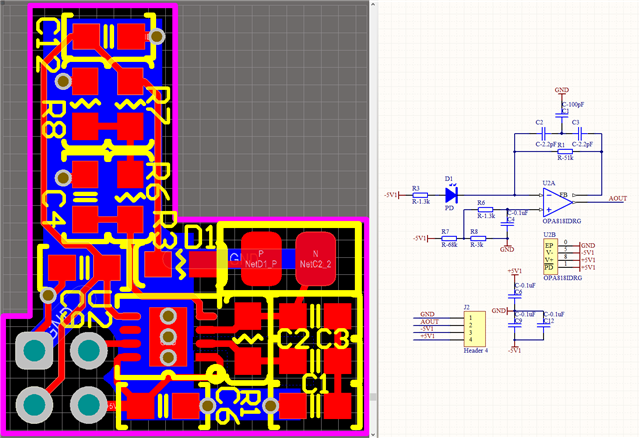
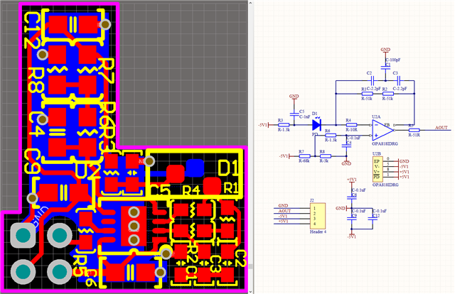
On the second version of the PCB (in order to reduce the parasitic capacitance, the board thickness was changed to 1.4mm), Rf was connected in series with 20kR and 30kR resistors (to reduce PCB area, the resistor was changed to 0402 footprint), no feedback capacitor installed, and the bandwidth was only 14MHz.

Both the chip capacitance and the photodiode capacitance have been tested, the chip capacitance is consistent with the nominal capacitance, and the junction capacitance of the photodiode is about 0.7pF under bias voltage. The bandwidth of the optical signal itself is above 50MHz.

There are the following questions:

  1. Why is the performance of the second version of PCB not as good as the first version?
  2. Does increasing PCB thickness (1.0-1.6) help reduce parasitic capacitance? Or is the impact negligible?
  3. Does changing the 0402 device to the 0603 device help reduce the parasitic capacitance? Or is the impact negligible?
  4. There is a big difference between the bandwidth calculated according to the formula and the actual measured bandwidth, is GBWP lower than the actual nominal value?
  5. How to reduce the parasitic capacitance?
  6. How to increase bandwidth without reducing transimpedance?

  • Hello Liu,

      Thank you for sharing this detailed analysis. The datasheet example is applicable in simulation. The TIA calculator snippet from the datasheet design shows 0.092pF feedback capacitance which is very difficult to achieve in practice as seen from the parasitic contributed from the PCB. We usually recommend aiming for a CF of >= 0.1pF or greater for transimpedance designs. 

      Your design choice of a capacitor feedback tee network does help with tuning the CF especially considering the parasitic and splitting the feedback resistor gain between two resistors is another good design choice for higher feedback resistor values to mitigate parasitic. 

      Some questions if you are open to a possible redesign with a higher bandwidth amplifier:

    1. To confirm, your photodiode capacitance is 0.7pF with your set reverse voltage bias?
    2. Your design needs a closed loop bandwidth of >50MHz 
    3. What is your input current range?
    4. What is your desired output voltage range? 

      Answers to your questions:

    1. This could be due to the addition of the isolation resistor R4. This resistor does help with parasitic inductance and capacitance. For now, try replacing it with a 0 ohm resistor. 

    2. Board thickness is negligible, but layer thickness is more important. From our test engineer, it depends on how far away the nearest planes or signal layers are away from each other (the spacing between these layers). When changing to a thicker board, is this only changing the center fill or the spacing between signal layers? Also, their suggestion is if you incorporate plane cutouts appropriately (input and feedback pins), then board thickness is negligible. 

    3. Yes, decreasing the passive size (Rf and Cf) would definitely help especially for sub 1pF designs. 

    4. GBP is the gain bandwidth of the amplifier and closed loop bandwidth is your system desired bandwidth (0.35/ rise time of your input pulse) 
      1. Calculator can be found at this link.

    5. Plane cutouts, reducing trace length to a minimal (which you have done), and passive component sizes 
      1. Kai has in-depth and very helpful advice in these threads
        1. https://e2e.ti.com/support/amplifiers-group/amplifiers/f/amplifiers-forum/1089964/opa855-q1-output-layout-instruction
      2. Stability in simulation
        1. https://e2e.ti.com/support/amplifiers-group/amplifiers/f/amplifiers-forum/1102658/opa858-tia-configuration
        2. https://e2e.ti.com/support/amplifiers-group/amplifiers/f/amplifiers-forum/1095982/opa855-opa855

    6. Changing to a faster amplifier (higher GBP, gain bandwidth product)

    Thank you,
    Sima