A related question is a question created from another question. When the related question is created, it will be automatically linked to the original question.
If you have a related question, please click the "Ask a related question" button in the top right corner. The newly created question will be automatically linked to this question.
You cannot apply a voltage source directly to an inverting input (pin 2) of an op amp unless you want to use it as a comparator. Under such condition, the output will be pushed close to its negative (V-).
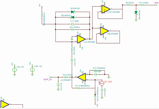
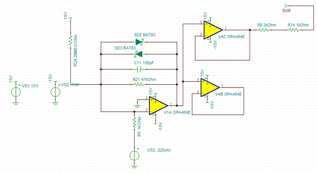
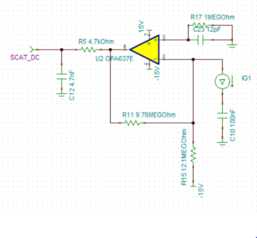
Attached the actual circuit image. The input to the SUM circuit is from the trans impedance amplifier(OPA637) output SCAT_DC of voltage 12.2V as per the simulation result with current input of -10nA at IS1.
Let me first say, your schematic is very difficult to read so there may be some errors in the component values I used below.
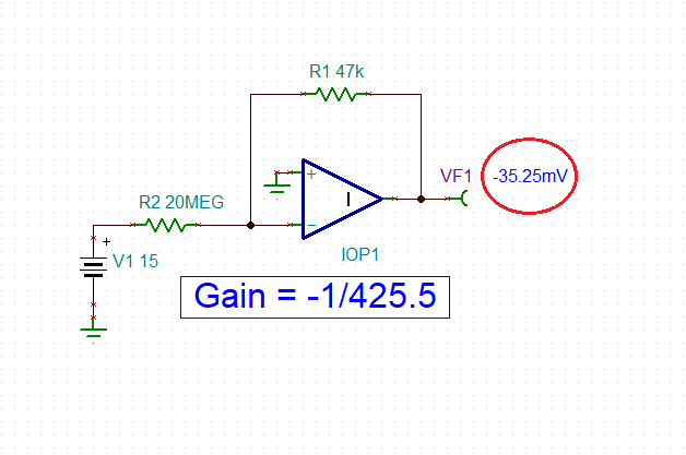
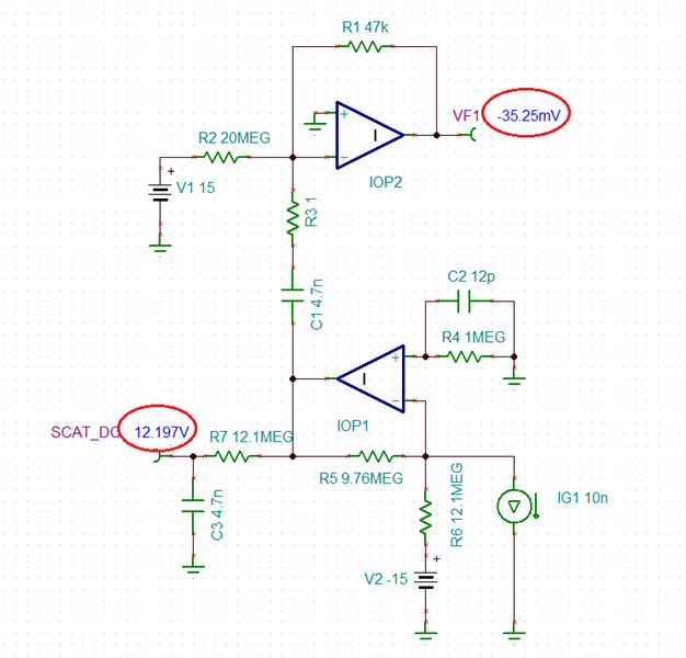
From the DC perspective, lower circuit (OPA637) plays no role since it is isolated by C14 cap - thus, the upper op amp is simply in an inverting gain of G=-1/425.5 resulting in the VF1 = V1*Gain= -15V/425.5 = -35.25mV - see below.
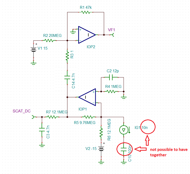
You say that with current input, IG1, of 10nA, you read SCAT_DC voltage of 12.2V BUT you cannot have DC current that is AC coupled (C10) like you show below because this would cause the input of IOP1 (OPA637) to saturate at the positive rail (a non-linear operation).
Thus, the circuit could only work with no C10 cap as shown below.
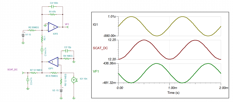
To say anything about the circuit response beyond its DC operating point shown above, one must provide information regarding IG1 AC input signal.
For example, using IG1 of 1uA at 1kHz, results in the output shown below.
Below I have attached Tina-TI schematic for your own simulation.
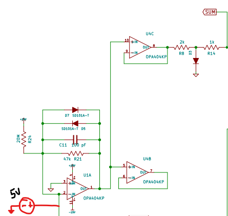
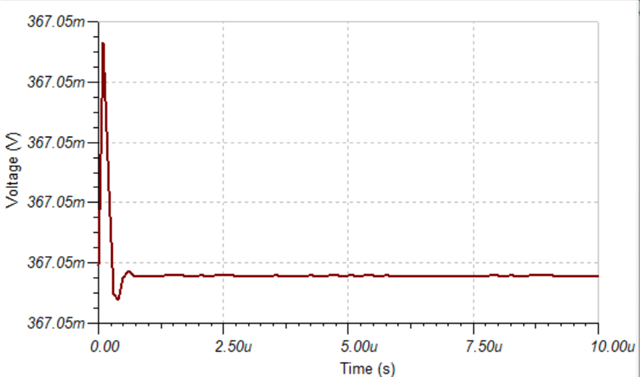
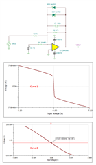
Attached the actual SUM circuit and its response. Please tell how this opamp reponds with Schottky diode and Capacitor at the feedback. Is this an integrator circuit?
Also, regarding the below circuit input, Its both DC and pulsed.
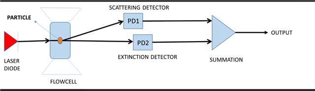
Attached the application circuit for reference.
The output of the photodiode will be proportional to the input light, so constant light would produce a DC signal, and oscillating light would produce an oscillating signal. So this will depend on laser diode.