This thread has been locked.

If you have a related question, please click the "Ask a related question" button in the top right corner. The newly created question will be automatically linked to this question.

LM393: device behavior question

Part Number: LM393

,Hi,

Please refer to beloe circuit.

My customer design Vcc is 3.3V, so the IN+ and IN- should be lower than Vcc-2V=1.3V

The IN+ and IN- in the design is 3.3V, according below statement 4, when IN+ and IN- (3.3V) higher than common-mode (1.3V), output should be low, is that correct?
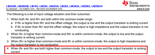
  • That statement is correct. But please note that outside the valid input range, the electrical characteristics (especially propagation delay) are no longer guaranteed.

    For low-voltage applications, better use a low-voltage comparator with rail-to-rail inputs like the LM393LV.

  • Hi Jim,

    As Clemens mentions, it is correct and I would also refer you to LM393LV which is well suited for low voltage applications and pin compatible with LM393

  • Thanks Clemens and Nguyen.

    I’m confuse, common-mode is 1.3V, when IN+ and IN- are 3V, that outside the valid input range so the function is not guaranteed.

    But according to the statement, IN+ and IN- are higher than common mode, output should be low.

    I mean how to hit the condition of the statement, it must be outside the valid input range.

  • Hi Jim,

    When both inputs are outside the common mode, the "expected" behavior is that the output will go low. But because the common mode range is being violated, the performance is not guaranteed. Please see section 2.2- 2.5 of this app note to understand about the input structure of this family:Application Design Guidelines for LM339, LM393, TL331 Family Comparators (Rev. C) TI can only recommend operating within the input voltage range. 

    Please note that LM393 is undergoing PCN and that for the new die, the output will actually go high. This is also mentioned in the app note. I would highly recommend using LM393B so that you are aware of any issues that may occur. 

  • Hi Chi,

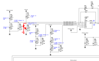
    Please help to check below schematic modify and excel calculation, we change divider resistance and the circuit should work, right?

    Any problem of the modification?

     LM393 power good latch calc.xlsx

  • Hi Jim,

    Chi is currently out of office, so I will be assisting you with your issue.

    Could you send another screenshot of the schematic that includes the pull-up resistor values at 1OUT and 2OUT of the comparator? These values are important in the calculation of the comparator's hysteresis.

    In addition, you will need to remove any capacitors connected to ground in the nets PG_COMP_P3V3_AUX_IN+ and PG_COMP_P3V3_AUX_2IN+ (C1188 and C1190 in the image). Capacitors in the comparator’s feedback network work against hysteresis and creates a delay in the feedback path.

  • Hi Siu,

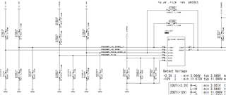
    Please have schematic, please help to check, thanks.

    BTW, C1189 and C1191 at IN- are OK to install, right? All need to remove as well?

    PQ4000E_IOB_R03_schematic_20230531_P121.pdf

  • Hi Jim,

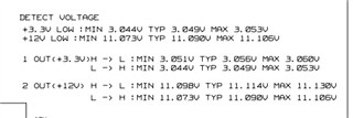
    From the resistor values you have selected, your channel 1 would have hysteresis values of VL = 2.97V and VH = 3.29V. For channel 2, you have hysteresis values of VL = 10.78V VH = 11.76V. VL and VH are the switching thresholds for the output of the comparator from high to low and low to high respectively.

    C1189 and C1191 are fine to keep since they are not on nets that affect hysteresis.

    Attached are images of the transfer characteristics of your circuit.

  • Hi Siu,

    Thanks for your reply and simulation.

    Looks like the CH1 VH=3.29V and CH2=11.76V are too close to 3.3V and 12V, I'm afraid the comparator output may not work as expected if any input source (3.3V or 12V) are not precise.

    If I want to make CH1 and CH2 VH lower, I have to reduce CH1 R3 and CH2 R8 resistance, right?

    For the VH and VL threshold, how is the tolerance? percentage? (max/typical/min value?)

  • Hi Jim,

    Decreasing the R3 and R8 resistances is one way of reducing VH, but keep in mind that the hysteresis of your circuit is a function of more than just R3 and R8. Since you are using an inverting comparator with hysteresis, you may refer to Analog Engineer's Circuit: Inverting Comparator With Hysteresis Circuit to help with your design.

    To find the variations in VL and VH from ideal, you will need to account the tolerances of your resistors. For the worst-case values, you will need to refer to the electrical characteristics of the LM393 to find the maximum input offset voltage and apply it to the positive input of your comparator. In addition, you will need to take the maximum input bias current over temperature and multiply it with the equivalent resistances at your IN+ and IN- nodes, then apply those voltages to the respective nodes.

  • Hi Siu,

    Thanks for the information.

    Could you please help to check below design and provide the resister value (R1~5 and R7~11) for both channel?

  • Hi Siu,

    Are you using TINA for simulation?

    Customer can not find the device in TINA.

    Could you please provide your file as well let customer try?

  • Hi Jim,

    Our team is out today and tomorrow July 4th holiday. We will take a look at this closely when we get back on Wednesday. 

    And yes we use TINA for simulations. Our models are located in the devices product folder under the Design and Development tab. Those have all new and updated tina and pspice models.

  • Hi Jim,

    Attached are two TINA files for you to use. Could you simulate them to confirm that this is the behavior that you want? Keep in mind that this is an idealized model of the behavior, and that it doesn’t account for nonidealities like input offset voltage, tolerance, and input bias current. In addition, you have a few degrees in freedom in altering the resistances per your tolerance and power requirements.

    From your specifications, it seems like you want a 7mV threshold window for your 3V3 monitor, and a 24mV threshold window for your 12V monitor. Keep in mind that these windows are small, and the fact that you are using a voltage divider to maintain common mode requirements scales these windows down.
    JimTsai3V3.TSCJimTsai12V.TSC

  • Hi SIU,

    Please help to check below schematic/TSC and VL/VH setting.

    1. 3.3V: VL=2.94, VH=3.067

    2. 12V: VL=11.04, VH=11.16

    Please help to check whether the resister are correct, thanks.

    PQ4000_P3V3_final_solution.TSCPQ4000_P12V_final_solution.TSCPQ4000E_IOB_R03_schematic_20230710_P121.pdf

  • Hi Jim,

    The transfer characteristics and transient simulation look good to me. I'm going to note that the simulated values might not be the exact values that you've stated here, but they are close enough such that it should be fine. For example, the simulated value for 3V3 is VH = 3.07V and VL = 2.92V. I’ve edited the timestep of your transient simulation so that you can see the simulated values better.

    I also noticed that the capacitors on the feedback path (C1188 and C1190) on your updated schematic have not been removed yet. As suggested before, it’d be best to remove them as to not add delay to your feedback path.

    PQ4000_P3V3_final_solution_updated.TSC PQ4000_P12V_final_solution_updated.TSC