This thread has been locked.

If you have a related question, please click the "Ask a related question" button in the top right corner. The newly created question will be automatically linked to this question.

Variable Gain Amplifier

Other Parts Discussed in Thread: THS3001, THS3091, VCA824, THS7001, VCA821, VCA820, VCA810, VCA822, OPA695

Hi

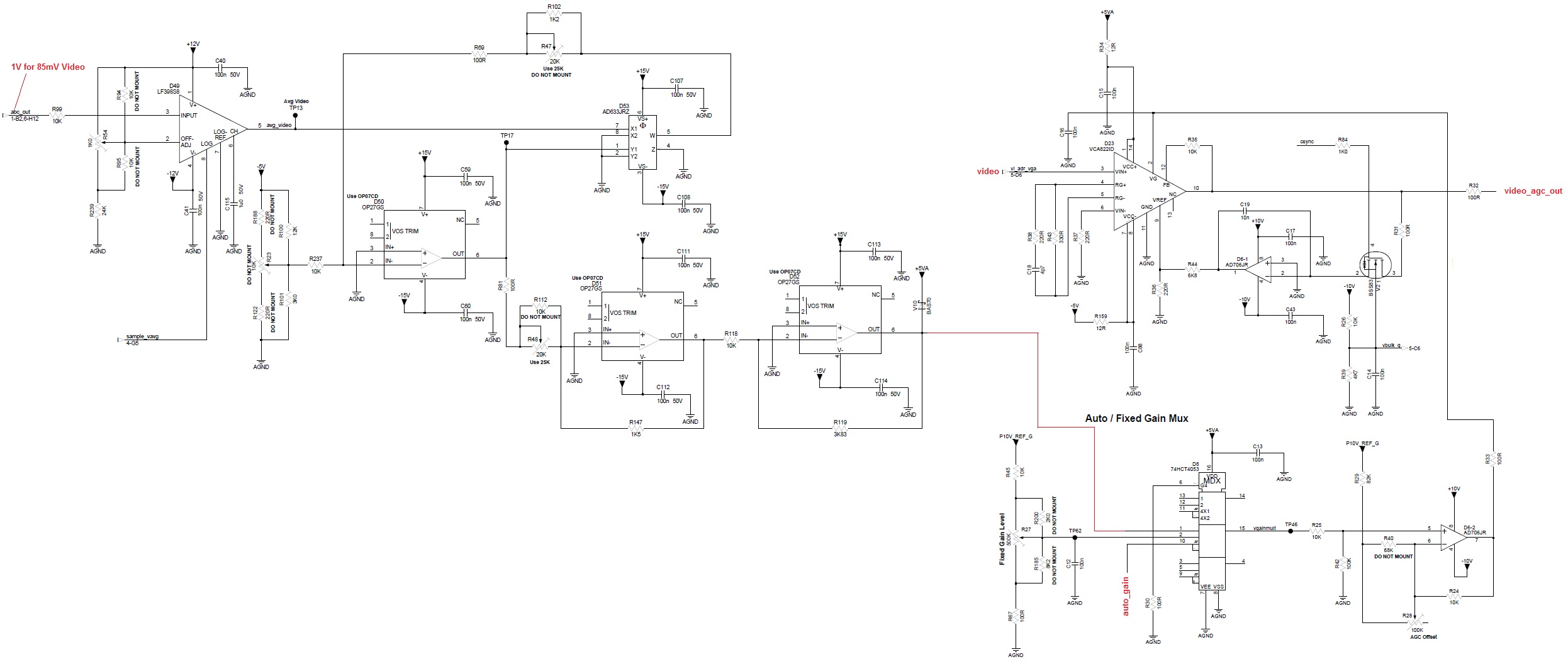
I would like to design a variable gain amplifier using a current feedback amplifier lie the THS3001. Is it possible to change the value of the gain resistors in circuit without causing problems. I am thinking some kind of analog switch to select different values. Or would this be considered a bad idea. If any body has any other thoughts on how to do it then that would be great.

TIA

Jon 

  • Jon;

    Yes, that is a bad idea; current-feedback amplifiers' feedback resistors are part of their frequency compensation. If you deviate from their optimum value, your frequency response will be over-damped or under-damped, possibly to the point of oscillation. You can, however, use a THS3001 in a fixed noninverting gain and vary the attenuation of a voltage divider at its input..

  • There is usually an optimal value of Rf for current feedback amplifiers, so switching that resistor value is a bad idea.  Also, both ends of the Rf resistor are sensitive to parasitic reactance. 

    The Rg, though, is quite flexible and consistent performance over a large gain range is a strong point for CF op amps.  The challenge is finding a way to change the value of the gain set resistor without introducing undesirable parasitic capacitance - especially at the inverting input of the amp.  Parasitic capacitance on the ground side of Rg is not as much of a problem, especially if it is capacitance to ground. 

    One possibility would be to use FETs to connect the different gain set resistors to ground.  Close only one FET at a time to select the gain.  You'd have to test this to make sure that the unconnected resistors didn't load the op amp input too much.  A passive analog switch could possibly do the same thing.

    One other possibility is to use an analog multiplexer to pick taps from a resistive divider.  A 4:1 analog mux could offer 4 gains.  There are analog multiplexers offered with current feedback output buffers and programmable gain. 

  • Let me reiterate-- adding gain switches to high bandwidth current feedback op amps is fraught with peril. Added parasitic capacitance on input nodes will very likely cause instability and oscillation even if the recommended gain resistors are used. If you still wish to proceed, try using a very small geometry DMOS transistor such as an SD211 as a switch. It has extremely low capacitance but its ON resistance will still need to be considered.

  • Jon,

    I agree with the comments posted on this thread as it gets a bit tricky swichting gain around in a device like the THS3001. But I want to add a couple more comments and ideas.

    There is the trade-off between optimum performance and the value of RF that varies with gain, and capacitance at the negative input of the device needs to be as small as possible (less than 1pF is best). But if you do not need the maximum slew rate and bandwidth at all gains and the gain variation is not too much, you may be able to find a tradeoff that meets your needs. Refer to table 1 on page 19 of the data sheet for recommended values. Keeping the capacitance low enough at the inverting node is a bit trickier. I have not seen anyone implement this approach so I cannot give a positive recommendation.

    An easier and more common approach to designing a PGA is to use a switched attenuator stage followed by a fixed gain amplifier. The amplifier is placed in the maximum gain desired and the input signal is taken from different attenuation steps or taps of an R2R ladder (R2R is usally used because it gives constant input impedance). A critical element of the design is the interaction of the switch capacitance with the ladder resistors, because as you move up and down the ladder, the RC changes causing variations in phase delays and can limit the bandwidth. If this is not critical, you may be able to implement something with discrete components keeping in mind the swicthes need to be linear and able to handle the frequencies of operation. If it is critical, I would look to an integrated device like the PE4302 from Peregrine, which may be overkill for your requirements, but Google "programable attenuator" and you can see lots of parts.

    Another approach is to use an integrated PGA device like the THS7001, VCA810, VCA820, VCA821, VCA822, or VCA824. These can provide an up front vaiable gain function and follow with the THS3001 in fixed gain to get the signal amplitude up to where you want it. Also note you may want to look at the THS3091 for improved performance drivng high amplitude signals into low loads.

    I hope this helps. If not, send more detail on bandwidth, signal amplitude, slew rate, noise, gain, distortion, power supply voltages, etc, and we can try again.

  • Here are some Tina simulation files to illustrate the 3 approaches described in last post. The first 2 show OPA695, which is a lower voltage CFB like THS3001, but faster, and the file has some parasitic capacitors added. The 3rd file is with THS3091.

    6710.OPA695 VGA Switch Feedback 6-8-2011.TSC

    8130.OPA695 VGA attenuator 6-8-2011.TSC

    6320.VCA824_THS3091 9_10_11.TSC


    TI-Tina is free. For more information and download link go to  http://www.ti.com/tool/tina-ti 

  • Jim,

    I use VCA822 for video AGC. Below is the portion of the schematic. The basic requirement follows:

    A DC feedback voltage is generated proportional to the average value of the video amplitude, whose value = 1 when the video amplitude = 85mV. Whenever the video amplitude is above 85mV the VCA822 operates at a fixed gain of 1 (control voltate fed from potentiometer). The AGC mode gets activated when the video amplitude is below 85mV. The control voltage for VCA822 is generated using a divider (1/x function). The requirement is to operate upto a gain of +10V/V. That is, if video amplitude is  42.5mV the gain shall be 2, at 21.25mV g = 4, at 14.17mV g = 6, at 10.62mV g = 8, at 8.5mV g = 10 etc. so that always the output shall be at 85mV. I'm not able to achieve this with the below shown component values for VCA822. From the datasheet it's not clear how to determine the component values (R35, R37, R43, R38, C18) for the required Gain Vs. Control Voltage characteristics.

    I don't have a thorough understanding of the above circuit since I do not own the complete design. And I don't have the design calculation too. I tried with TINA simulation example. But it's not giving the expected results for the component values given in the datasheet under section TYPICAL CHARACTERISTICS: VS = ±5V, AVMAX = +10V/V (page 13).

    Kindly assist.

    Thanks | Sinoj