This thread has been locked.

If you have a related question, please click the "Ask a related question" button in the top right corner. The newly created question will be automatically linked to this question.

OPA817: How to avoid crosstalk between different analog channels?

Part Number: OPA817
Other Parts Discussed in Thread: THS4551,

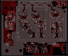
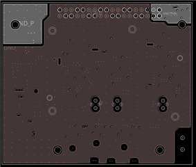
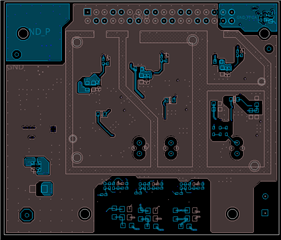
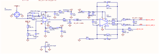
I'm designning a board including three channels of light pulse detection, each channel contains OPA817 and THS4551 as following:


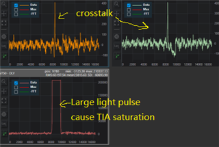
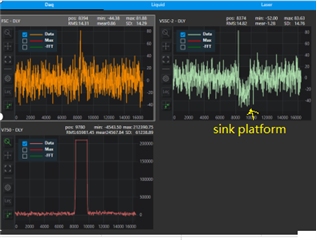
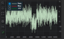
During test, I found large pulse on one channel will cause some crosstalk on other two channles. Adding metal sheilding between each channel can suppress the crosstalk but still need to improve.

I'v removed the light sensors on other two channels and tested again and the crosstalk still existed. With furthere tests I believed they are caused by both radiation and circuit conduction.

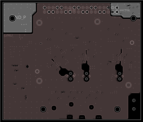
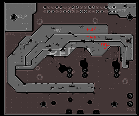
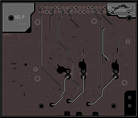
So I want to seperate the three channels as much as possbile but wondering what is the reasonable way. I imagined one scheme to seperate the power and GND on this board. 

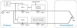
(Both posstive and negative rails are separated but not shown in the pic)

Does it make sense? But if I add metal sheilding between different channels and connected the sheilding to GND, the separation of GND seems useless.

Who can share some ideas and detailed notice on handling the similar problems?

BR,

Thanks!

  • Hi Follin,

    The separation of supplies and ground planes might offer some benefit, but the source of crosstalk is most likely due to signal traces interacting. Designing and laying out a PCB with multiple planes might not offer as much benefit for the added complexity.

    Here are some quick design tips for suppressing crosstalk:

    Reduce the length that two lines are allowed to run in parallel. A minimum spacing of three times the signal width is a good rule of thumb.

    Be sure to have solid return paths where possible. Reducing the separation between signal and ground ensures the signal has a good return path. Ensure you still maintain the expected trace impedance.

    Use guard traces with vias connected to ground.

    Keep traces in adjacent layers perpendicular to each other. Signal traces running parallel in adjacent layers can also cause significant crosstalk.

    I also attached a TI article that gives more details on different considerations and PCB layout tips to reduce crosstalk. The article has applicable information to help reduce the crosstalk issue you are experiencing. The article can be found here.

    We can also take a look and review the layout of the PCB and offer suggestions.

    Best Regards,

    Ignacio

  • Hi Ignacio,

    Thanks for your advice! And here's the layout. If you can leave me a mail addrees I can send you some doc for easy to check.

    L1 TOP

    L2 GND

    L3 POWER

    L4 Signal

    L5 GND

    L6 BOTTOM

    The frame shape on the top and bottom are the bared copper for metal sheilding assembly.

    I've read the artical you post. And I find one thing is that I use wide trace for each power  on the power layer, shall I use single plane for each power to make it better?

  • Hi Follin,

    Having a complete power plane would offer its benefits like the article highlights, however after looking over your layout the design seems like it is well isolated. Your signal paths for each channel do not look like they would be interacting with each other too much considering the spacing between them. What level of crosstalk are you experiencing/measuring? How much did the metal shielding between the channels help comparing the measurement with and without?

    Best regards,

    Ignacio

  • Hi Ignacio,

    Here are some test result of with or without shielding. Large light pulse goesing in to channel A's APD and other two channels have no light sensor.

    Without shielding: The peak of the crosstalk would be around 5mV

    With shielding: The peak of the crosstalk would be around 1mV

    But the light pulse is not as large as in the final use case. In the final use case, the peak of crosstalk (with shielding) will be around 3mV.

    And there's a obvious sink platform when the channel A TIA gets saturated.

    I've also tried decreasing the other two channels gain resistor (from 470k to 50k), the crosstalk also got smaller. But I need the large gain.

    And at this case, the sink platform still exists, that's why I doubt the spike is caused by Radiation but this platform is caused by circuit Conduction. 

    But I've filtered each power supply for both positve and negtive rail so currently I'm at a loss for what to do next.

  • Hi Follin,

    I have sent you a private message so we can continue our discussion.

    Best Regards,

    Ignacio