This thread has been locked.

If you have a related question, please click the "Ask a related question" button in the top right corner. The newly created question will be automatically linked to this question.

THS4551: filter design and front end circuit

Part Number: THS4551
Other Parts Discussed in Thread: OPA810, TINA-TI, ADS127L11

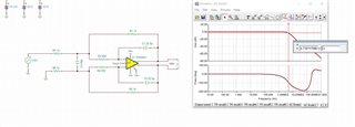
Q1: if need to increase filter from 500K to 5M, how to change filter part value?

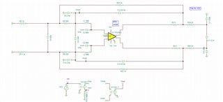
Q2: Is OPA810 circuit necessary? Can we remove it? Any other recommendation OP for bandwidth 5M?

Q3: Just refer to oscilloscope front end circuit, can C1 and C2 capacitor be removed if resistor divider on the same PCB? I suppose it’s only need for oscilloscope probe because of probe wire capacitance.

front end schematic.pdf

  • Hello Liping,

    1. You can do something similar to these values in the below Tina-TI simulation. The 5 ohm isolation resistors internal to the capacitor feedback loop can be kept, but I would change them to 0hms to start, and up the value if you run into instability. 

      Below is transient analysis of the FDA with around 5MHz -3dB cutoff frequency. Filter values would need to be changed if you require passband up to 5MHz and increase cutoff frequency
         

      Below is stability analysis of the FDA with the same filter values. It is around 42 degrees with the 5 ohm isolation resistors which is at the brink of stability. To increase stability, I suggest increasing gain and adjusting the input voltage divider to OPA810. Or, keeping and tuning the noise gain shaping input capacitor as you have included in original schematic, C4. 


      However, I do recommend checking the voltages at the input of the FDA. With a +/-5V single ended input to the FDA at single supply configuration, you will run into a common-mode violation. I recommend biasing the input common-mode voltage. 

    2. Yes, a FET-input is necessary for a high input impedance design due to your need to attenuate a high voltage signal. A FET-input amplifier has low bias currents which decreases voltage offset errors. Also, your design would need a RRIO amplifier which is one of the specifications of the OPA810. However, I would adjust the voltage to slightly below +5V and above -5V for 150-200mV headroom at output. 

    3. Will this design be used for a oscilloscope scope front-end application?

    Thank you,

    Sima

  • For question 1, the reference design comes from datasheet of ADS127L11. Can you tell more about the C1, C2, C3, C4 and later 22nF close to ADC.

    We have so many filters, but why we can not combine it?

    For question 3, I just design for voltage measurement like oscilloscope. But we dont' use any probe in my application.

    It means CH1 will be connected to measurement point through a wire directly. So can we remove capacitor at input resistor divider?

  • Hello Liping,

       C1, C2, C3, and C4 are part of the multiple feedback topology (MFB) using a fully differential amplifier (FDA). The MFB provides a 2nd order filter + filter response which in the above case the values were picked for Butterworth response for a flat passband. The filter at the output provides another filter (in total 3-order filter) and acts as a charge bucket filter prior to the ADC. Higher order filters will provide stepper attenuation at the cutoff frequency which can lead to better noise overall. Also, the charge bucket filter has shown to improve SNR and THD. 

       References below:

    1. Design Methodology for MFB Filters in ADC Interface Applications
    2. Using the infinite-gain, MFB filter topology in fully differential active filters
    3. ADC charge bucket filter 

      Yes that is correct, if you have DC input design with no need for switching to AC coupling, then you can remove the capacitor. 

    Thank you,
    Sima