


Other Parts Discussed in Thread: LOG114, OPA3S328
Optical power monitors are necessary for real-time network performance reporting of signal strength and integrity in telecommunication systems. A typical optical power monitoring scheme uses a photodiode as current source; this current source is fed into a transimpedance amplifier to deliver a voltage that is to read by an ADC. Amplifiers with wide input current range, fast setting times, and small form factor are much needed for these applications. Texas Instruments has taken an innovative solution and has released the LOG200 specifically for optical power monitoring.
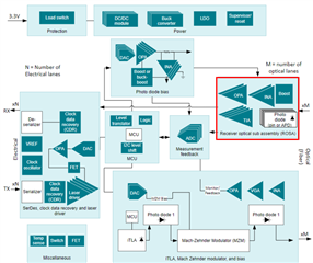
Figure 1: Optical Modules Reference Design
Benefits of Logarithmic Output
- Easily spans across multiple decades of current with good resolution
- No inherent crossover region/uncertainty associated with a switched gain amplifier
- Optical power is measured in decibels, preventing the need for a conversion stage
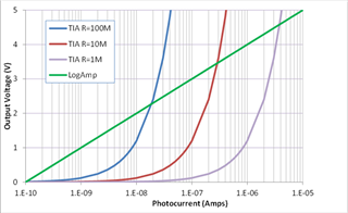
Figure 2: Logarithmic vs Non-logarithmic Output Reading
What is the LOG200?
The LOG200 is the industry’s fastest, high-precision logarithmic amplifier and features a 120 kHz bandwidth at 1nA of input current, ±1% gain error, and ultra-fast response times. With a rise time of 0.22 µs and a fall time of 0.63µs to a 10-100nA step, the LOG200 will be able to quickly detect changes in optical power across many decades of current. The LOG200 has built off its predecessor, the LOG114, and has improved on key specifications including extended temperature range in a smaller footprint.
Device |
Input Current Range |
Log Conformity Error |
Gain Error(25°C) |
Step Response 10nA-100mA(µs) |
BW at 1nA(kHz) |
Temperature Range (°C) |
Package Options |
|
LOG114 |
100pA – 10mA |
0.2% (1nA-100A) |
±2.5% |
1.5 |
5 |
-5 to 75 °C |
4x4mm 16 QFN |
|
LOG200 |
100pA – 10mA |
±0.2% (10nA–100A) ±0.5% (10nA–1mA) ±0.75% (1nA–10mA) |
±1% |
0.22 rising 0.63 falling |
120 |
-40 to 125 °C |
3x3mm 16 QFN |
Optical current sensing is the main focus of the LOG200. The following image shows how to configure the LOG200 using 5V supplies and a current range of 10nA to 100uA.
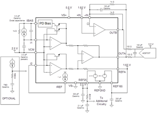
Figure 2: Typical Photodiode Current Sensing Application with LOG200
Non-Logarithmic Amplifier Solution
In the case where a log amp is not necessary, a reliable and high performing transimpedance amplifier can still be used, such as the OPA3S328. This dual precision CMOS amplifier offers low noise, high bandwidth, and low input bias current, as well as integrated switches for programmable gain which is optimal for transimpedance applications.
For a detailed description on how to use the OPA3S328 in your design, visit the following link.
Building a Transimpedance amplifier with the OPA3S328
Device |
Voltage Range (V) |
Bandwidth(MHz) |
Noise at 10kHz(nv/√Hz) |
Input Bias Current (max) (pA) |
Operating Range (°C) |
Package Options |
|
OPA3S328 |
2.2 to 5.5 |
40 |
6.1 |
10 |
-40 to 125 °C |
3.5mmx3.5mm 20 VQFN |
The simplified circuit diagram shown in Figure 3 shows a programmable gain Transimpedance amplifier circuit implemented with the OPA3S328. The OPA3S328 integrates analog switches useful to select the TIA gains across multiple decades of photodiode current. The second-stage amplifier buffers the programmable gain TIA stage using Kelvin sense connections to eliminate errors due to the switch on-resistance, switch resistance drift, and non-linearity. This allows for the design a low noise, high bandwidth, high accuracy programmable gain TIA to perform optical power measurements.
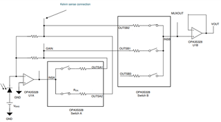
Figure 3: Switch Kelvin Sense Connection and High Impedance Buffer for Photodiode Current Sensing
-By Nicholas Rubalcaba
