This thread has been locked.

If you have a related question, please click the "Ask a related question" button in the top right corner. The newly created question will be automatically linked to this question.

LMH6554: Single-ended to differential conversion application information discrepancies

Part Number: LMH6554

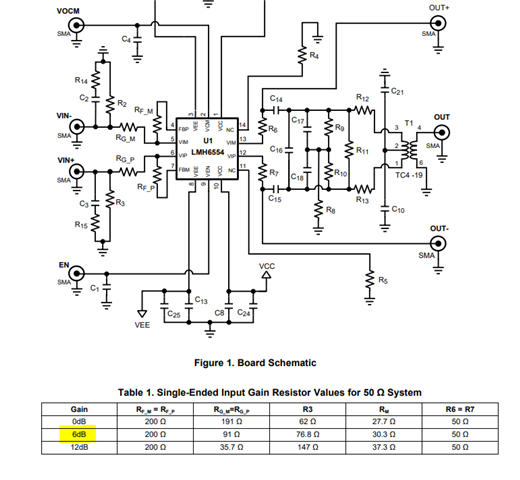
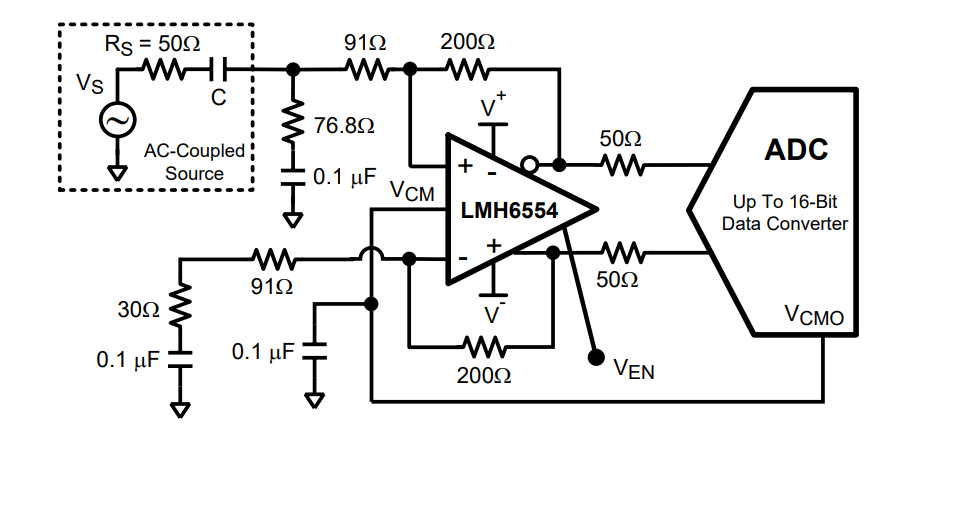
I'm following the guidelines from the LMH6554 datasheet and the evaluation board sheet for my design. I realized there are a couple of discrepancies in the application information for single-ended input to differential output conversion on page 15 of the datasheet and page 1 of the evaluation module guide. The resistance R_T that is mentioned in the calculations of the datasheet doesn't show in the board schematic of the evaluation board, so does this resistance correspond to the parallel equivalent of R_3 and R_15? What about the capacitance? Finally, the evaluation board sheet claims that one should use the capacitor C_3 for AC coupling but then it recommends using the VIN- input is this correct or a typo?

  • Hello Bastien,

      You may use either input or both inputs on this EVM. If you would like AC coupling, it could be done on either or both inputs, but I do agree that the user guide suggests using VIN- directly after suggesting C3 for AC coupling which is a typo. It should have been consistent and recommended either input or VIN+ input right after that statement. 

    Thank you,
    Sima

  • Hello Bastien,

     Correction to the above reply. VIN- is correct since C2 and R14 = OPEN and you would have to use a AC coupled source. Then, the user-guide suggests populating C3 and R15 for balancing.

      Also, under single-ended input mode of operation, EVM user guide suggests:

    "For single-ended input mode of operation, the input and termination resistance must be properly configured to give the correct gain and input impedance (RIN). For example, in the case of the LMH6554, if a gain of 2 V/V is desired, R2 = R3 = 76.8 Ω, RG_M = RG_P = 90 Ω, RF_M = RF_P = 200 Ω, C2 and R14 = OPEN, C3 = 0.1 µF, and R15 = 50 Ω, which will make RIN = 50 Ω at the most positive node of R3 looking into RG_M."

      You can treat either R2 and R3 as the R_T in this case depending on which input you are driving. Or if grounded and whichever input is left floating, it would be the parallel combination of the two input resistors (i.e. R_3 and R_15) as you mentioned. 

      For example. let's say you want to single-ended input and you are driving VIN+ for a gain of 2V/V. Then as shown in the snippets below: 

      You would follow the recommended resistor table under a gain of 2V/V for a 50 ohm AC coupled VIN+ source (dotted box in second image shows source is AC coupled and has 50 ohm impedance). 

       R3 is your RT which is 76.8Ohms, and Rm is the parallel combination of R2 and R14 (50//76.8 = 30.3 Ohms). VIN- is left floating (do not connect to ground). 

       If your VIN+ source is DC coupled (50ohm), then short across C2 for balance. 

    Thank you,
    Sima