This thread has been locked.

If you have a related question, please click the "Ask a related question" button in the top right corner. The newly created question will be automatically linked to this question.

LMV7275: LMV7275MG/NOPB design review

Part Number: LMV7275
Other Parts Discussed in Thread: TLV9020

Hi,

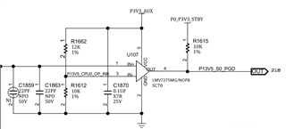
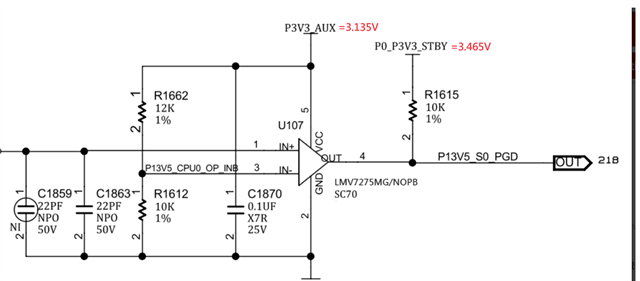
I would like to use LMV7275MG/NOPB design as below schematic, could you please help to review and provide your comment.

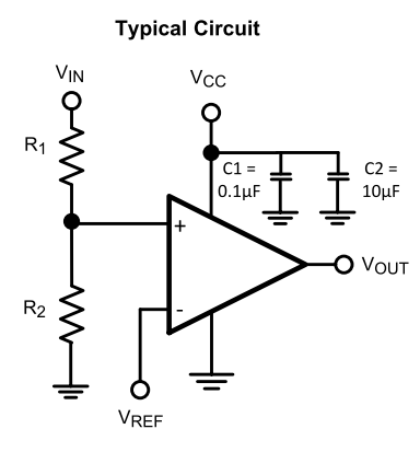
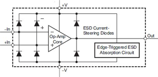
Do you have relative OP design and need to check portions? If you have,could you share for me?

Thanks, 


  • Another question, if IN+>IN-,the output is open drain, so output is P0_P3V3_STBY, right?

    VCC needs 10uF for LMV7275MG/NOPB? Our schematic is only 0.1uF for VCC, this design is ok or not?

  • Hello Danny,

    Your circuit looks fine, as long as the input voltage is between 0 and 3.3V. at pin 1.

    Yes. When the output is "high" the output voltage will be the pull-up voltage (P0_P3V3_STBY), or. 3.3V.

    0.1uF at the supply pins should be fine, as long as there is a larger capacitor on the rail as part of the rest of the system.

  • Hi Paul,

    Thanks. VCC needs ready before IN+,right? If IN+ voltage >VCC voltage, is there any impact? 

    Thanks,

  • Hello Danny,

    Ideally, V+ should come up before the inputs.

    Even though the LMV7275 is an open collector output, it does have an upper ESD diode clamp from the output to V+, so the output cannot exceed V+.

    So if V+ is at 0V, and the pull-up voltage is present, the pull-up will be clamped by the ESD diode to the V+ rail.

    The result will be an output of about 600-800mV during that time, or you could end up slowly back-feeding the comparators V+ supply through the ESD diode (if the V+ line is lightly loaded).

    Also, the inputs will also be clamped to the V+ rail, and could similarly back-feed the comparators V+ supply if the input voltages are present.

    It's best to have the V+ supply come up first.

  • Hi Paul,

    Thank you. VCC(P3V3_AUX) come up before IN+ in our design.

    If we consider component tolerance, and VCC is 3.135V and ouput pull up to (P0_P3V3_STBY) 3.465V as figure, is there any risk ?

    Another question, if IN+ is 4V or 5V and larger than VCC pin, is there any risk ?


  • Hi Danny, 

    As Paul mentioned, there are internal diodes from the inputs and outputs to V+, so the output cannot be pulled higher than V+ and the inputs should not be larger than the V+ pin.

    I would recommend TLV9020 which is a drop in replacement with improved specs and features such as fail safe so the inputs can be above V+ without damage. The output can also be pulled above V+ up to 5.5V 

  • Hi Chi,

    Could you provide LMV7275MG/NOPB internal ESD(diode) spec? I would like to study it.

    What is it's breakdown voltage ? Because our design is IN+ around 3.7V and larger than V+ (3.3V) , but this LMV7275MG/NOPB is from customer request, if we would like to change this solution, and need to inform customer why need to change TLV9020 in our application.

    Thanks,


  • There is no breakdown. When the input voltage is larger than V+, a current will flow normally through the diode. This current, if not limited, might burn out the diode and anything nearby. The absolute maximum ratings forbid voltages larger than (V+) + 0.1 V.

  • Hi Paul and Chi and Clemems,

    So TLV9020 doesn't have internal ESD diode between input and V+ and between output and V+, right?

    Thanks, 

  • Hello Danny,

    Yes. The inputs only have a "snapback" diode to V- to allow the inputs to go up to 6V, regardless of the supply.

    This is all explained in section 7.4.3.2 of the datasheet.