This thread has been locked.

If you have a related question, please click the "Ask a related question" button in the top right corner. The newly created question will be automatically linked to this question.

OPA455: Error in "Detailed Design Procedure"?

Part Number: OPA455
Other Parts Discussed in Thread: OPA462

Hi,

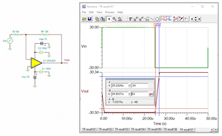
On the OPA455 data sheet, the slew rate is given as 32V/us. but in the Design Procedure (Section 8.2.1.2), it is said to be only 6.5V/us.  Can I assume that's a typo?  I'm pretty clear on the rest of the data sheet, but concerned I might be misunderstanding something in 8.2.1.2.

There's a pretty much the same issue in the OPA462 data sheet as well.

  • Hi George, 

    On the OPA455 data sheet, the slew rate is given as 32V/us.

    You are correct. Thanks for pointing out the typos in both datasheet's Section 8.2.1.2, where full power bandwidth calculation examples are presented. I will make a note of these.

    For OPA455, the slew rate (SR) is specified at 32V/usec. For OPA462, the SR is also rated at 32V/usec, which are specified in the datasheet section.

    In addition, the SR feature can be simulated via Spice model, which the simulated example in OPA455 is shown below.  

    OPA455 Slew Rate 11102023.TSC

    If you have other questions, please let me know. 

    Best,

    Raymond