This thread has been locked.

If you have a related question, please click the "Ask a related question" button in the top right corner. The newly created question will be automatically linked to this question.

ALM2403-Q1: Circuit stability

Part Number: ALM2403-Q1
Other Parts Discussed in Thread: ALM2402F-Q1, OPA564-Q1
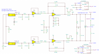
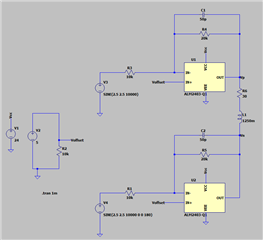
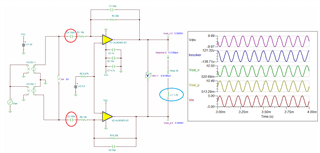
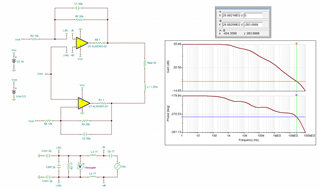
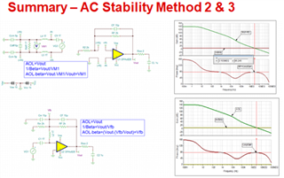
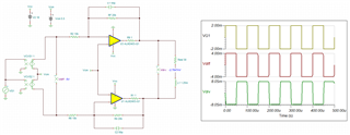
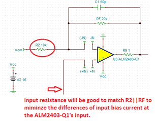
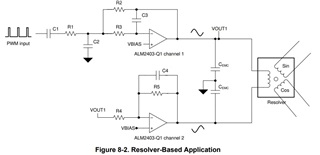
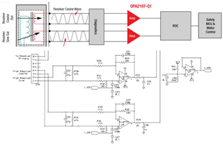
I want to use ALM2403 to design a circuit that drives the resolver, but because the resolver is an RL load, does TI have any documents that can help me confirm how to design the circuit to avoid circuit instability?

  • Hi Lin,

    does TI have any documents that can help me confirm how to design the circuit to avoid circuit instability?

    Enclosed lists below are the how to video series in stabilizing op amp closed loop in a typical application. For resolver load, the techniques are very similar, except the resolver load has R, L and C components, and the load is treated as a rotational transformer. 

    002559

    As in any op amp driving circuit, it is necessary to check for the loop stability. However, we will need to have a schematic first before we are able to simulate the load with the driver. 

    Please provide me with resolver's load parameters and the circuit design requirements. Without the schematic, it is difficult to discuss the circuit instability, if any. 

    Below is an example of resolver driver, but your schematic and load may be different from the example. Let us finalize your design first, then we can perform and check for the circuit stability analysis. 

    ALM2403-Q1 SPWM Input 12122023.TSC

    If you have other questions, please let me know. 

    Best,

    Raymond

  • Hi Raymond,

    I think the stability of the opa circuit should be the same as that of the dcdc converter. It needs to ensure sufficient phase and gain margin, is that right?

    If so, how should I set how much margin to keep?

    In the reference circuit, I think it is a 4th order filter. Does it need to be set to 4th order to filter out the internal sine wave?

    If my exc signal is a sine wave, do I still need to set it to the 4th order filter?

    Finally, there is the filter composed of R11, C6, R16, and C10 at the output end. Are there any requirements for the frequency design of this filter?

  • Hi Lin,

    If so, how should I set how much margin to keep?

    There is always a way to improve phase margin, but a circuit may or may not trade something for the loop stability. We will address the stability issues when we are reaching that point. The issue is that you have not finalize the resolver driving circuit, it is too early to talk about the loop stability. 

    Theoretically, the minimum phase margin needs to be great or equal 45 degrees. Typically, I would like to keep the phase margin at approx. 60 degrees or higher. 

    Does it need to be set to 4th order to filter out the internal sine wave?

    In the example, I use 2rd order LPFs to filter out 300kHz SPWM input signal, then I limited the BW of ALM2403-Q1 to 20kHz to further smooth out the remaining sinusoidal input and provide the differential output at the same time.

    I could also use active LPF to filter out the SPWM signals, but the example is to simplify the input stages for a user. You could make as elaborate as you want to be in order to meet the design requirements. In automotive application, costs are very sensitive and simplified design approach is desired, unless the application has other specified requirements. 

    Typically, 2nd-3rd order LPFs should be enough to filter out harmonics noises of typically SPWM signals, say 300kHz (depending on your SPWM's switching frequency), but the LPFs or sinusoidal smoothing approach depends on what the design requirements are called out.    

    Are there any requirements for the frequency design of this filter?

    These design components are used to center the output differential driving signal above and below GND reference. The added capacitances are to make R, L and C resolver load close to resistive behaviors, if the lead and lag of the phase current in L and C are closed matched or canceled, and leave the complex load behaves more resistively. This will improve the phase margin and improve the power factor of the resolver system.

    I would recommend to take apart the previous resolver simulation and simulate each part of resolver stage and modify the circuit that are suited for your design requirements.

    Enclosed link is another ALM2403-Q1 resolver design approach. For the automotive application, there are additional fault protection circuitries, which you need to consider. Once you have completed the simulated resolver design, we can address the resolver's loop stability and make the improvement. 

    If you have other questions, please let me know. 

    Best,

    Raymond 

  • Hi Raymond,

    This is the most basic circuit architecture.

    I need to know how to set up the filter connected to the resolver.

    My input is a sine wave. If I set the LPF at 20kHz according to your example, this will affect my gain.

    For this part, what is the reference for setting the range of the filter, for example, setting it to 5 times the input frequency.

    In this example, at 0db, the phase is about 119 degrees and the phase margin is about 60 degrees, which should be sufficient.

    Of course, the most important thing is how to judge the stability of the circuit. Please tell me how to judge it on this circuit.

  • Hi Lin, 

    From your attached simulation, your differential input signal is +/-5Vpk at 10kHz. If this is pure sinusoidal signal, the setup does not have significant switching harmonics except the fundamental. In this case, you may limit the ALM2403-Q1's BW at >100kHz or 159kHz per your simulation. 

    There are a couple typos. Your Voffset is configured at 5Vdc, so your DC bias at inverting input should configure the same or at 5Vdc, where AC is riding on top of 5Vdc. Alternatively, you can insert a capacitor to couple the input signals as shown in the simulation below. 

    The transformer's inductance is a bit high, which I think that it may be a typo. 1250mH is equivalent to impedance of 78537.5Ω (sL) at 10kHz. It is likely that this is 1.25mH instead. Please confirm that  your resolver's load parameters. Please provide me with the actual resolver load, not hypothetical one, since ALM2403-Q1 is limited to power dissipation. Typically, resolver may be able to handle the excitation current up to ±100-200mApk @10kHz, which ALM2403-Q1's average heat dissipation is approx. 2W. We have to consider the normal operation at a worst case in temperature condition. For automotive application, the worst case Tamb operating temperature is at approx. 85C to 100C.   

    If you have other questions, please let me know. 

    Best,

    Raymond

  • Hi Lin,

    Let us assume the inductance is 1.25mH instead of 1.25H, below is the AC stability analysis. Since you mentioned the stability analysis inquiries in multiple occasions, I demonstrate the loop analysis method here. 

    Please keep in mind that this is generally the last step, because you did not include all the necessary circuitries in the simulation. In the resolver, there are winding capacitance, which we ignored. There are short circuit protection circuitries we did not include. And I do not know if ALM2403-Q1 is capable to drive your resolver load under all Tamb operating conditions, which Tamb is typically up to 85C to 105C for automotive application, depending on the design requirements.  

    For the simplified resolver load, the phase margin is approx. 76 degrees (360 -  283.7 degrees).

    ALM2403-Q1 Dual AC Analysis 12142023.TSC

    In TI's precision op amp video training series, which I posted in the previous reply, the method 2 on he bottom stability image is prescribed. The method 3 on the top stability image is basically the same as method 2. Anyway, I post this slide here FYI. 

    To verify the small signal step transient stability analysis, below is the example, where no overshoot is shown and the circuit is stable. 

    ALM2403-Q1 10kHz Step Transient Analysis 12142023.TSC

    BTW, I am unable to support LTSpice simulation due to the license agreement. In the LTSpice, you may use opamp2 to generate the op amp symbol for the simulation, which is more readable. 

    If you have other questions, please let me know. 

    Best,

    Raymond

  • Hi Raymond,

    I made a mistake here: the inductance value is 1.25mH. Another issue concerns the DC bias.

    According to my simulation results, it seems to be normal. Will there be any problems if the setting does not exceed 5Vdc?

    The coupling capacitors C4 and C5 appear to act as high-pass filters. What problems might arise if I do not set these capacitors?

    Another concern is about the DC bias terminal resistor R2. I read in TI documents that it's recommended to set this resistance value to be the same as the input resistance value of ALM2403, but I can’t find the value of the input resistor in the datasheet. Could you please provide the input resistor value?

    Lastly, there is the simulation result of the Bode plot. The gain appears to be around 55.6dB, whereas the DC gain I set is about 2 times, which is 6dB. This seems to be a bit different. What could be the reason?

  • Hi Lin, 

    According to my simulation results, it seems to be normal. Will there be any problems if the setting does not exceed 5Vdc?

    ALM2403-Q1 has a wide Vcm input range, therefore, you can set anywhere within the Vcc or supply rail. Typically, users wound like to configure the Vcm at the mid rail of a Vcc, and configured the Vcm with two equal value in a resistor divider. The Vcm range is determined by your output voltage swing and the minimum Vcm requirements. 

    Vcm will not be good to set near at the minimum, since there will be no design margins. For a typical resolver with output sinusoidal swing at 7Vrms or greater, the Vcm should be configured at minimum 5Vdc. In the AC analysis example, I configured at 5.5Vdc to provide it with the extra design margins. In the recommended example, Vcm is configured at 1/2 * Vcc. The ALM2403-Q1's output is a differential driver, and Vcm in DC does not enter the transfer equation, as long as Vcm on both end of primary winding of the rotational transformer is equal and tracking. 

    Could you please provide the input resistor value?

    I think that R2 is referred in circled red, see the comments below. 

    The gain appears to be around 55.6dB, whereas the DC gain I set is about 2 times, which is 6dB.

    6dB refers to closed loop gain. During AC loop stability analysis, loop-gain T, is plotted out, which T = Aol/Acl. In log term, it is LogT = logAol - logAcl. 

    The coupling capacitors C4 and C5 appear to act as high-pass filters. What problems might arise if I do not set these capacitors?

    Yes, this is a way to look at it. The excitation frequency is operating at 10kHz, You may increase C4 and C5 to move the poles to a lower frequency. Since you are using the pure sinusoidal  10kHz input, it makes sense to increase the capacitance value to 1uF - 10uF. Or you may use my simulated approach and bias the sinusoidal 10kHz to the Vcm, which I configured it at 5.5Vdc.  

    I'd like to point out that ALM2403-Q1's input can be wither in sourced from inverting or noninverting input. There are Pros and Cons in either design approach. In the recommended example and design approach, Vcm in DC at the output of differential outputs are fixed and does not change. Since the application is driving a transformer, this design approach has the advantage, where AC is riding on DC Vcm. The transformer does not work in DC, therefore, the DC biasing voltage at the input of excitation transformer will cause the constant DC across the transformer's input terminals, and no DC current will flow within the primary winding, and magnetic saturation in the transformer core will be minimized. 

    If you have other questions, please let me know. 

    Best,

    Raymond

  • Hi Raymond,

    I think I already know that when AOL is equal to 1/β, phase_AOLβ must be greater than 45 degrees to ensure circuit stability.

    But in the example ALM2403-Q1 Dual AC Analysis 12142023.TSC you provided me, why is it not measuring the voltage across Rresolver but measuring Vloopgain?

    As mentioned at the beginning, what are the recommended values ​​for the design of the filter capacitor Cemc connected to both ends of the resolver?

    Or do I just need to set the filter point I want and ensure that the circuit is stable?

    Finally, the example at the beginning is ALM2403-Q1 SPWM Input 12122023.TSC.

    How can I adjust it in the circuit so that it can simulate the stability of the circuit?

    You can also see that the example circuit uses 2 opas, but what we are discussing now are circuits with one opa.

  • Hi Lin,

    You can also see that the example circuit uses 2 opas, but what we are discussing now are circuits with one opa.

    Please provide your resolver design requirements and application. I am unable to read your mind what the design requirements are. I will be happy to recommend the best design approach, if I know the design requirements and application. Typically, resolver or rotational transformer is driven as a floating load, which it requires two op amps that drive a resolver differentially. 

    why is it not measuring the voltage across Rresolver but measuring Vloopgain?

    I have suggested a systematic design approach to work on your project. You have insisted me to show you how to "Of course, the most important thing is how to judge the stability of the circuit. Please tell me how to judge it on this circuit." That is the reason that I discussed the loop gain with you. As I mentioned in multiple times, the resolver driver's AC stability analysis (or loop gain analysis) is the final design phase of a resolver design. 

    As mentioned at the beginning, what are the recommended values ​​for the design of the filter capacitor Cemc connected to both ends of the resolver?

     I do not recall that you are ever mentioned about the capacitive coupling at the ends of the resolver. You mentioned the capacitive coupling at the inverting input of the ALM2403-Q1, which it has nothing to do with the capacitive coupling at the end of the resolver. 

    Yes, there are two ways to couple ALM2403-Q1's differential output to the excitation winding of the resolver's primary. One is direct coupling approach, which it includes DC + AC signal (this is the one that I have simulated above). The other method is to use 2 capacitors to capacitive couple the resolver's primary winding. Both coupling methods will work, but it depends on your design requirements. 

    Please provide your resolver design requirements for your application. Without the design requirements, I have no ideas what you want. 

    The support teams are going to enter the holiday seasons shortly (some engineers may have started already). Please provide your complete design requirements, so I can help your design issues quickly. I won't be back to office after the first week of the new year. There will not be anyone who is able to support your inquiries during the holidays. These are the reasons that I am replying to your inquiries over the weekend. 

    If you have other questions, please let me know. 

    Best,

    Raymond 

  • Hi Raymond,

    My design requirements are very simple.

    Originally I used the AD2S1210 IC. The application circuit in this IC uses OPA+BJT to form a buffer circuit.

    Now I want to use ALM2403 to replace the OPA+BJT circuit.

    As you can see, the recommended circuitry within the AD2S1210 is much simpler compared to that within the ALM2403.

    In contrast to your initial example, there's an added high-pass filter at the input and an RC circuit (comprising R11, C6, R12, C10) connected to the Resolver winding.

    This led me to inquire about the principles behind selecting this RC combination.

    You mentioned it's to make the resolver behave more like a resistor.

    From that, I speculate that it's meant to generate RLC resonance in the output load, allowing the LC components to cancel each other out, mimicking a resistance-like behavior in the load.

    However, I'm still uncertain about how to simulate the entire circuit to verify if the load behaves as a resistor.

    Since the stability circuit we're currently discussing is a simplified version based on the recommended circuitry in the AD2S1210, I also want to understand how I should simulate stability regarding the example you provided.

  • Hi Lin

    Now I want to use ALM2403 to replace the OPA+BJT circuit.

    ALM2403-Q1 is designed with two power amplifiers or 2 of Figure 27 buffer circuits in a single package. Since ALM2403-Q1 is a MOSFET process, the output power buffer stages are designed with the complementary mosfets. Both power amplifiers are designed in 5mm x 4mm in HTSSOP (14) package.  If this is what you are looking for, then ALM2403-Q1 can readily replace Figure 27 circuit with an additional power amplifier to spare. In the similar resolver product lines, we have ALM2402F-Q1 and OPA564-Q1, which are well suited for the resolver application. 

    Regarding to the resolver's design requirements, here are the minimum design requirements that I'd like to know.  

    a. Input excitation frequency signal -> you mentioned that it will be 10kHz analog sinusoidal waveform. (if the input is SPWM, please specify)

    b. Input 10kHz analog frequency's amplitudes

    c. How many input lines are there? one or two lines of excitation differential input signals (digital or analog)

    d. What is the Vcm of the input signal? 5.5V or others. 

    e. What are the input LPFs requirements? RC LPFs or Active filters etc.

    f. What are power amplifier's gains and cutoff frequency? (op amp's BW requirements)

    g. What are output sinusoidal excitation voltage swing (typically resolver's output stage needs swing up to 7Vrms @10kHz)?

    h. Resolver's L, C and R parameters --> you mentioned ESL = 30Ω,  L = 1.25mH@ 10kHz and  may be up to 10nF of the resolver primary winding capacitance.

    i. Resolver shall be driven differentially or floating or driven the resolver load directly GND.

    j. How the resolver shall be coupled at the output stage of the ALM2403-Q1 (direct coupled or capacitive coupled at the resolver's input terminals). 

    k. Are there any fault protections required at the output of the ALM2403-Q1, such as output terminals shorted to GND or shorted to Vehicle's battery etc.. 

    l. What is the application's operating temperature range? say -40C <= Tamb <= 100C and the worst Tamb is 100C or higher. 

    m. What is the power supply rail available for the ALM2403-Q1 resolver application?

    n. Any cost requirements of consideration?

    o. Any power efficiency consideration?

    If you are able to provide me the above design requirement, I will be able to provide the best design approach for the application, and perhaps I will recommend some options. 

    If you have other questions, please let me know. 

    Best,

    Raymond

  • Hi Raymond,

    a. Input excitation frequency signal -> you mentioned that it will be 10kHz analog sinusoidal waveform. (if the input is SPWM, please specify)

    Basic 10k, maximum 20k.

    b. Input 10kHz analog frequency's amplitudes

    0~5V

    c. How many input lines are there? one or two lines of excitation differential input signals (digital or analog)

    2,0~5V and 5~0V

    d. What is the Vcm of the input signal? 5.5V or others. 

    Vexc_in is 0~5V,the offset voltage is 2.5V, Vcm is 6V.

    e. What are the input LPFs requirements? RC LPFs or Active filters etc.

    Base on the exc frequency is 10kHz,I want to set the LPF as 10k*7~10 times.Do you have any better suggestions?

    f. What are power amplifier's gains and cutoff frequency? (op amp's BW requirements)

    DC gain is 2.3.There is no idea with opa's BW requirements.

    g. What are output sinusoidal excitation voltage swing (typically resolver's output stage needs swing up to 7Vrms @10kHz)?

    7Vrms,10kHz.

    h. Resolver's L, C and R parameters --> you mentioned ESL = 30Ω,  L = 1.25mH@ 10kHz and  may be up to 10nF of the resolver primary winding capacitance.

    I only have the parameters fot RL.

    i. Resolver shall be driven differentially or floating or driven the resolver load directly GND.

    Differentially.

    j. How the resolver shall be coupled at the output stage of the ALM2403-Q1 (direct coupled or capacitive coupled at the resolver's input terminals). 

    Previously, it was directly connected to the resolver. I'm curious about the differences between the two approaches.

    k. Are there any fault protections required at the output of the ALM2403-Q1, such as output terminals shorted to GND or shorted to Vehicle's battery etc.. 

    NO.

    l. What is the application's operating temperature range? say -40C <= Tamb <= 100C and the worst Tamb is 100C or higher. 

    worst temp is 85degC.

    m. What is the power supply rail available for the ALM2403-Q1 resolver application?

    24V.

    n. Any cost requirements of consideration?

    NO.

    o. Any power efficiency consideration?

    NO.

    Thanks a lot.

  • Hi Lin,

    Thanks for providing the design requirements. When engineer asks for an open ended questions, I do not know what is the best answer to address these questions, because there are many considerations and/or options. 

    Regarding to the analog input stage and ALM2403-Q1 filter choice, here is one of the suggestion. The ALM2403-Q1's BW is limited to 159kHz range and you should not see a significant amplitude attenuations from input signals. Since the input is ±10Vpp, the ALM2403-Q1's gain can be configured for -1 V/V.

    10kHz filter 12182023.TSC

    In terms of resolver driver circuit, here is the basic driving configuration. The output will meet the 7Vrms @10kHz voltage swing requirements. 

    ALM2403-Q1 10kHz Resolver Driver 12182023.TSC

    Previously, it was directly connected to the resolver. I'm curious about the differences between the two approaches.

    The ALM2403-Q1's power amplifier output stages are fairly well matched, so the there are no significant voltage biasing at the primary winding of a resolver. So we can use direct coupling as shown in the simulation above, and resolver's magnetic will not be saturated due to the design approach. 

    In many discrete resolver driver configuration, due to the mismatching of power amplifier driver stage, the DC biasing across the primary winding of a resolver may no be as consistent, and there may be a large voltage delta in DC across the winding. Under the such scenarios, the capacitive coupling may be more suitable. The capacitor will block the Vbias difference, and as long as the differential output driving signals are balanced, the resolver should not experience residual magnetism  shift or walk within the magnetic core of a resolver, therefore the magnetic core (BH curve) will be reset in each cycle during operation. 

    In terms of AC loop stability, I performed the Loop Analysis in the previous reply and it should apply to the same circuit. 

    Below is ALM2403-Q1 EVM, which you may purchase from digikey.com or mouser.com. You may modify the EVM and get the resolver running rather quickly. 

    https://www.ti.com/lit/ug/sbou236a/sbou236a.pdf?ts=1702930284032&ref_url=https%253A%252F%252Fwww.google.com%252F

    Please let me know if this is what you have in mind. We can make additional changes from the baseline design. 

    Best,

    Raymond

  • Hi Raymond,

    Thanks a lot,I will learn more.

    In addition, the resolver circuit actually includes sin and cos feedback.

    It is a complete set of applications. Doesn't TI have an EVM board for sin and cos feedback?

  • Hi Lin, 

    I am glad that this helps. 

    The resolver driver is feed forward driving architect for the resolver's primary winding. The negative feedback is placed at the output of the power amplifier or at the input terminals of resolver. So are the sine and cosine return lines. Assume the magnetic link is near 100% coupled (treat it as ideal transformer at 10kHz), the secondary windings of the sine and cosine coils are simply proportional to the turn ratios. No feedbacks are needed for the resolver application. the coupling losses can be negligible for the operating frequency.  

    The ALM2403-Q1 EVM is only addressing how the resolver's primary winding is driven. The secondary windings in sine and cosine coil interfaces are not addressed on the board. 


    If you want to know about how to capture sine and cosine in the 2nd windings, please check out the links below. 

    https://www.ti.com/lit/wp/spry212a/spry212a.pdf?ts=1702947357861&ref_url=https%253A%252F%252Fwww.google.com%252F

    https://www.ti.com/lit/ta/sszt365/sszt365.pdf?ts=1702947589650&ref_url=https%253A%252F%252Fwww.google.com%252F

    If you have other questions, please let me know. 

    Best,

    Raymond

  • Hi Raymond,

    As you know, I'm using the AD2S1210 IC, which requires differential inputs for its feedback sin and cos signals.

    I cannot sum these before inputting them into the AD2S1210, so I need to design circuits for processing sin_p, sin_n, cos_p, and cos_n separately.

    Typically, RC filtering introduces some delay.

    Therefore, I'm aiming to design a circuit with minimal delay after RC filtering. Ideally, I need a design that employs pole-zero cancellation.

    Does TI have any documentation on using OPA filters and designing for pole-zero cancellation?

  • Hi Lin,

    I cannot sum these before inputting them into the AD2S1210, so I need to design circuits for processing sin_p, sin_n, cos_p, and cos_n separately.

    Yes, you have to amplifier the sine and cosine signals first. The schematic below is shown how the difference amplifiers are implemented to obtain sine and cosine secondary windings information. You have to gain up the signals first before you sample the waveforms. The image is in the first application note that I posted. 

    Does TI have any documentation on using OPA filters and designing for pole-zero cancellation?

    Do you have a circuit in mind? This is an open ended question, and I do not know how to answer it properly. In our precision op amp video training series, the topic are mentioned numerous times, please see my previous video links. In order to maintain the op amp's stability with adequate phase margin, an op amp's roll off needs to be maintained at -20dB/decade across the unity gain bandwidth. Please revisit these video series. 

    If you have other questions, please let me now. 

    Best,

    Raymond

  • Hi Raymond,

    As shown in the diagram, the sin and cos signals are intended to enter the IC in a differential mode.

    This is an example circuit.

    Here is the simulation circuit.

    You can see the phase delay of the circuit is 18.8.

    In addition to providing the gain adjustment, the receiver circuit also acts as a third order Butterworth filter with a cutoff frequency of 63 kHz and a phase shift of −18.6° at 10 kHz.

    The simulation results are almost identical to the description in the documentation.

    I believe phase delay in handling the sin and cos signals could be a significant concern, potentially causing the motor angle derived from the IC to lag.

    Therefore, I need to advance the phase to prevent severe phase delays.

  • Hi Lin, 

    Please keep in mind that I can only support you if you are using TI parts. I am unable to support you with competitive op amps. 

    Please contact TI's FAE in the field and we can discuss your project further. 

    Best,

    Raymond

  • Hi Raymond,

    I knowed.

    I just want to know the formula of butterworth filter.

    Because TI also has an online filter calculation tool ANALOG-FILTER-DESIGNER.

    I need to move the offset of the sin and cos feedback signals first, and then design the filter.

    I need to know how to adjust the design.

    As I asked at the beginning, TI does not seem to have a reference design or document for resolver feedback signal.

    Of course you have provided me with a copy, but I cannot actually use that circuit design.

  • Hi Lin,

    The E2E forum is supported via US site, and we are currently in holiday recess due to Christmas and New Year holidays. 

    To answer your question, here is the site that you may be able to get what you are looking for a different filter configuration. 

    http://sim.okawa-denshi.jp/en/MultipleFB3Lowkeisan.htm

    As I asked at the beginning, TI does not seem to have a reference design or document for resolver feedback signal.

    Here is the reference design for the resolver feedback signals. It is simply a difference amplifier. 

    Best,

    Raymond