This thread has been locked.

If you have a related question, please click the "Ask a related question" button in the top right corner. The newly created question will be automatically linked to this question.

INA190: Oscillation of Switch cap frontend

Part Number: INA190
Other Parts Discussed in Thread: INA186, , THS3120, INA193

Hello,

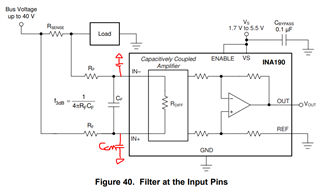
I would like to know what options may exist for the INA190Ax using the SOT23-8 package inside TI's current sense amp or instrumentation amp which would allow me to design out the INA190Ax and still stay in the SOT23-8 package. I have the oscillation problem mentioned in other threads and my noise is not high (<30mVrms on 1.8V). I see the INA186 uses the same pinout for same function but this device still has the cap coupled front end (switch cap) and my application does not have the differential mode input filter in the layout (ughh). Is there any part (instr amp or Curr sense amp) which might work in this application. (e.g. same pinout SOT23-8 and same function)?

  • Hello Appreciated Engineer,

    I am looking this over and will respond shortly.

    Sincerely,

    Peter

  • Hey Thomas,

    Could you describe what this noise issue is? I cannot find the aforementioned thread.

    Also what is the common-mode voltage requirement for you system?

    Other requirements such as IQ, gain, BW, error, and sense current range (low and high) would be extremely useful to narrow down the search.

    Sincerely,

    Peter

  • Hey Thomas,

    Here are the available current sense amplifiers and instrumentation amplifiers that are in the same SOT-23 package:

    https://www.ti.com/amplifier-circuit/current-sense/analog-output/products.html#2954=SOT-23%3BSOT-23-THN&sort=236max;asc&

    https://www.ti.com/amplifier-circuit/instrumentation/products.html#2954=SOT-23-THN&sort=2954;asc&

    Not sure if this would work, but here are the digital current monitors we have in the same package:

    https://www.ti.com/amplifier-circuit/current-sense/digital-power-monitors/products.html#2954=SOT-23%3BSOT-23-THN&

    There are no difference amplifiers nor fully differential amplifiers in the same package.

    Most other devices will not have similar input capacitively-coupled front end as the INA190 has so as long as the orientation of the pins is the same (and other device specs meet system requirements), then you will have a suitable alternative.

    Sincerely,

    Peter

  • Hello the common mode voltage is 1.8V and the noise is thought to be resonance of the INA190A2 when operating at this Vcm with a periodic 'noise' from a shunt current monitored SMPS. I believe the noise is periodic between 600kHz and 1.6MHz and has a spectrum whose largest energy lies within that band. My thought is that is interacting with the 'capacitively coupled' frontend of the INA190A in such a way that the amplifier output is resonant. I have decided to purchase the INA190Ax EVM board which has a 190A2 and I will connect that to an wide band amplifier (your THS3120 EVM board) easily capable of driving the INA190A2 with a 0.1 ohm shunt to close to the same operating point as my product. An Arb Gen will produce a periodic signal atop the Vcm of 1.8V and If I see resonance on INA190A's output then I will conclude I have problem with the INA190. The layout followed the guidelines of the INA190 however it did not have the PI filter on input pins or the post output filter for 'high noise applications' recommended in the datasheet. This is because our application was not considered high noise (<30mVrms atop 1.8V). We see the resonance in out ADC data only intermittently and also I have not concluded the problem is not downstream in the FIR digital filter yet either but I am looking at this simultaneously.

  • Hello Thomas,

    What could be happening is that the load current actually contains some periodic noise and this is what is causing the output noise. 

    Although 30mVrms of Vcm ripple at 1 MHz could easily be causing up to ±12 mV output noise as well for INA190A2. I calculate this by noting the input AC CMRR at 1MHz to be 45 dB (Figure 11). Vout_pk_pk noise = SQRT(2)*30mVrms*10^(-45dB/20)*Gain.

    And this calculation is probably an underestimate given that this Vcm ripple has energy over 600 kHz to 1.6 MHz.

    Finally, all amplifiers will have limited AC CMRR at 1 MHz, so  if this is the root cause, then you need to either incorporate and input filter with common-mode capacitors and/or an output low-pass filter with acceptable cutoff frequency or choose an amplifier with sufficient AC CMRR at 1 MHz.

    Overall, in order to determine root cause, you need to be able to test the INA190 with only a differential input pi filter and then with a differential filter and common-mode filtering capacitors (Ccm). When choose input capacitors, use the following rules:

    1. RF < 1kΩ to avoid significant input filter error. See datasheet for information on how to calculate this.

    2. CF (or Differential capacitor) should be chosen such that signal BW is not affected (fc = 1/(2*2*pi*Rf*Cf)  > signal BW). 

    3. Ccm <= Cdiff/10. You want the differential signal to dominate over changes in common-mode time constants to avoid dynamic offset error when Vcm is charging/discharging Ccm capacitors.

    Sincerely,

    Peter

  • Peter, Thanks for the response. First, I am stuck with my layout as it is now. I cannot add the CM or DM caps you have outlined. Regrading the "break into oscillation" that I described above, I should detail this more. I am seeing the data from our ADC break into an oscillation from a nominal noise result. This is to say that I see nominal 3 ADC counts peak-peak leap to about 30 counts pk-pk and then diminish back down to the nominal 3 ADC cnts pk-pk for the remainder of the time. Assuming the actual sampled current under measurement has not done this (and we believe this to be the case) is it possible that the INA190A2 has started into a broken into a resonance of 10x the nominal signal before and after the resonance has recovered to the nominal value of 3 cnts pk-pk?? -Tom I will post the .PNG showing this to your email since I cannot post using this E2E interface for some reason. 

  • Hey Thomas,

    While I wait for your image, can you measure the input Vcm signal (voltage between IN+ and GND) at the same time this oscillation event occurs? I would like to be certain that there is not some changing noise condition at input voltage causing a feedthrough to the output.

    Sincerely,

    Peter

  • Hello Peter, I have sent you a image of the data at 100Hz output rate to the email you provided. The figure shows 1KHz but I think the actual data is coming out at 100Hz (sorry). The FIR filter has a corner freq of around 250Hz and sample rate of 11.8kSps and is 64 tap. I will try to get a better view of the data (tighter timescale). Filter is catching large resonance spikes coming-through or caused-by the INA190A2 then we should be able to see that in the response even at such a low output rate. As you can see the possibility of aliasing is large here. I will be able to get more data from this setup very soon. 

  • Hey Thomas,

    I am looking over you data now.

    Best,

    Peter

  • Hey Thomas,

    It looks like the jump in output noise is occurring right after a power up (load power up) condition. Is this true? If so, is the load current jumping up from 0A immediately before the leap in noise occurs?

    I ask this because it is possible that if INA190 input is starting at 0mA, and then jumps, there could be some output oscillation. I have only really seen this when the device is starting with an overdrive condition (e.g., Vshunt = -10mV) and then input jumps quickly up. You could test this by applying a small reference voltage to REF pin (e.g., 50mV to 100mV) and then repeat the test. The reason this happen is when the input voltage switches during at the same time internal capacitors are switching at a specific point in sequence.

    The other possibility here is that you need a low pass filter (or charge bucket) in between INA190 OUT and ADC, especially for a SAR ADC. This could be causing instability by itself or be making the aforementioned possibility worse by adding load capacitance. The ADC datasheet does mention that it recommends the amplifier driving it be a buffer or a low-output impedance source, which the INA190 is neither.

    Try evaluating what is possible root cause by simplifying your circuit one variable at a time until this behavior ceases. For example, either disconnecting ADC and/or inserting a op amp buffer or RC filter (e.g, 400-Ω and 1nF), or driving REF pin with small 50mV source, or finally try adding 1 nF differential input capacitor at input pins of INA190. I understand your system may not allow this, but at least you would potentially know or rule out a root cause.

    Sincerely,

    Peter

  • I can re-run the test but I did not see those spikes at start up since I started the scope after the ckt was in steady state. I think this really is an oscillation breakout. For our current PCB layout, I have no locations for; 1) INA190 input Pi (DM or CM), 2) INA190 output simple low pass or 3) additional buffer amp for drive of AD7490 ADC. Please note that this channel (1.8V VCCAUX Artix) appears to be the only current shunt channel (8 channels total) we see this 'voltage blooming or swells' on. All other channels seem to make good sense and seem to be noise bloom free. I have sent a list of the eight Shunt monitor channel details for this board to your email. 

    I would like to proceed with my INA190x2 EVM board test set up which is independent of the actual board with the ADC since it shows something like oscillation independent of my board. Also, it is very difficult to add any parts to the actual board. HOWEVER, I can hack in a Pi Fitler in front of the 1.8V VCCAUX INA190x2 amplfiier and I want to collect some data with that board to see if these resonances are 'tamed'. 

    I will later add a Pi Filter (50ohm x2 and 0.47uF) to the EVM board test to see if that tames the oscillation on the EVM INA190x2 board with my noisy input. Furthermore, I can sweep the frequency and noise atop the 1.8V voltage on the EVM board and see that I get different values oscillation amplitude on the INA190's output (blue scope trace). I will try to get some scope pics with mor detail.  -Tom          

  • Hey Thomas,

    I will wait for your data.

    If you are using 8 total INA190 circuits and only one ever has this noise bloom, then we might also want to look over any differences in layout among them.

    Sincerely,

    Peter

  • I am only using the (one) x50 INA190x2 on the EVM board. I would think the EVM board layout is probably fine. Please note (from above) that I have modified the INA190x2 EVM board to match my board's application (No frontend Pi filter or DM caps and no output filter). My shunt is 0.1 ohm as shown here in my setup. Also, here are the results from above setup


    The yellow waveform is the actual 1.8V rail (J02 Keystone lug) going into the EVM board before the R82 shunt.

    This is indicating the break into oscillation we have seen in our actual data though the amplitudes do not match and the data you have seen in the previous slide sent (not the test setup but the actual data from the board), Again, that data is at a greatly decimated rate and is 64 tap FIR filtered with no anti-alias filter in front of the ADC or INA190A2.  

    Also, you can see from the list below that I am using INA190x2 and x1 and also the (switch cap FE free INA193) and I have not seen current noise bloom on these channels 

    Px_CurrMon_Cfg.txt
    Name:	Rshunt	INA19x_Amp_typ	Voltage (Vcm)	Pi_Filter 	 
    
    28V_C	0.03	INA193		+28V		Yes (50ohmX2/0.47uF)
    3p5V_C	0.22	INA190A1 (x20)	+3.5V		NO 
    IMV_C	0.082	INA193		+28V		Yes (50 ohmX2/0.47uF)
    HTV_C	0.05	INA193		+28V		Yes (50 ohmX2/0.47uF)
    1p8V_C	0.1	INA190A2 (x50)	+1.8V (VCCAUX)	NO 
    3p3V_C	0.1	INA190A1 (x20)	+3.3V 		NO
    1p0V_C	0.015	INA190A2 (x50)	+1.35V 		NO 
    1p2V_C	0.2	INA190A2 (x50)	+1.2V 		NO 


    Furthermore, as you have pointed out, we should not drive the AD7490  ADC directly and should have a buffer amp to avoid small noise errors due to noise injection from the AD7490 but I think these will be very small noise voltages and would not be responsible for the larger swells we see.  

  • Hey Thomas,

    1. Can we confirm that the swells really do occur when load is already in a steady state? The data ADC counts data you show me, shows a load current starting from 0.

    2. Have you tried an A-B-A swap by swapping the abnormal INA190A2 with another INA190 from one of you other channels to see if the problem follows the original device (indicates root cause has to do with device marginality) or shows up on the new device (indicates root cause has to do with channel)?

    3. Also, are you saying that you are seeing the noise bloom in the recent oscilloscope shot of INA190A2EVM output? Because I do not see anything close to the ADC data you sent showing 58mAp-p noise. So to me this oscilloscope shot shows me that the noise bloom in not happening with the EVM measuring this load, but it is happening with the INA190A2 soldered onto your system measuring this load. 

    Perhaps you could swap your abnormal INA190A2 and the EVM INA190A2 to see where the problem goes?

    All I can say is what I would do which is:

    A. Try to replicate the noise consistently (is it due some specific system change, or is it truly random occurring at load and bus steady state)?

    B. If I cannot replicate it, I would try to figure out how to be able to detect it with an oscilloscope trigger set to any noise blips at OUT pin (ADC input) that exceed ~40mAp-p.

          B1. Make sure to probe with respect to or close to INA190 GND pin

          B2 Compare what the noise swell looks like compared to ADC data

          B3. Also probe Vin+ and Vs (with respect to INA190A2 GND pin) to see if noise swell correlates to any channel or supply disturbances

    C. During steady state, use a differential voltmeter (portable possibly) to measure for any voltage difference between INA190 GND pin and VCCAUX return.

         C1. Also try measuring the resistance between them when system is powered off.

         C2. Measuring the voltage difference with a differential scope probe could also be extremely valuable to ensure there are no sudden changes in voltage, which would indicate significant impedance between them.

    D. Try changing simple circuit variables as mentioned before such as removing connection to ADC and/or inserting filters.

    E. Perform A-B-A swaps with other devices and retest for behavior using the same scope trigger.

    Sincerely,

    Peter

  • Hey Thomas,

    I am going to mark this thread as resolved, but if you have any other questions, updates, or concerns please post back.

    Best,

    Peter