This thread has been locked.

If you have a related question, please click the "Ask a related question" button in the top right corner. The newly created question will be automatically linked to this question.

INA201-Q1: Voltage on Vin+ and Vin- pins during no current flow

Part Number: INA201-Q1
Other Parts Discussed in Thread: INA201

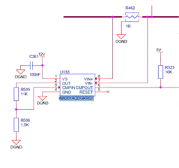
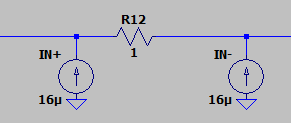
One of our designs uses INA201AQDGKRQ1 with the Vin+ and Vin- terminals connected across a 1R shunt resistor. During our built-in-test, there is no current flow across the shunt and the chip is powered by 12V. 

During the build-in-test we measure the voltage of both Vin+ and Vin- terminals, with reference to GND, to assure it is isolated form other parts of the circuit. 

Is there is voltage tolerance on Vin+ and Vin- that is documented during zero current flow across the shunt resistor? Or perhaps is there a leakage current value? 

See snippet of circuit attached.

  • Hey Patrick,

    Thanks for posting to the forum. We hope to solve and clarify your issues and concerns.

    Technically the device is not isolated from inputs pins. There will be leakage otherwise known as input bias current at the input pins that is dependent upon the input bus voltage. Table 7.5 has the specification for this listed out.

    Please follow up with any other questions you may have.

    Sincerely,

    Peter

  • Hi Peter,

    Thanks for the information.

    The datasheet states 'Input bias current, VIN– Pin '. Assuming this is just the value for the negative terminal. Is there a value for the VIN+, or will this be the same? 

    The bias current also states both +ve and -ve currents. Am I right the assume in my circuit that the inputs have the possibility of sinking or sourcing current? 

  • Hey Patrick,

    Of course sorry for lacking clarity.

    There is common-mode input bias current (IBcm) and there is sense current (Isense). When there is no shunt voltage (no Vsense), the input bias currents at IN+ and IN- pins will be equal, but variable to input common-mode voltage (Vcm). IBcm will go negative with negative Vcm. IBcm will probably shift slightly when Vcm < Vs.

    When Vsense > 0 mV, IBp will increase and IBn will stay the same. The total equation are

    IBp = IBcm + Isense

    IBn = IBcm.

    where Isense is approximately Vsense/6kOhm.

    Hope this makes sense.

    Sincerely,

    Peter

  • Hi Peter,

    Thanks again.

    For some context, I have simulated the full circuit to attempt to get a value for the 'zero shunt current' voltage we are reading during built-in-test. Using ~0uA bias current values on the IN+/IN- terminals gets a voltage value close to what the majority of our units are seeing, which is ~0.5V.

    However, we have some of our units float upwards to about 0.7V. We believe this is due to variances on the INA201 chip, as this was replaced and the voltage reduced. 

    Simulating with a current source of +3uA on both In+/In- leads to this 0.7V voltage value. 

    The datasheet states a maximum worst case of 16uA, so assuming that as worst case. See below snippet of how I have done this.

    Is this method of 2 equal current sources correct, assuming 0A sense current?

  • Hey Patrick,

    A positive 16µA would actually be going into the device pin (so the arrows would need to be flipped in you circuit). But yes this is essentially the equivalent to what the device is doing at 0-A load current.

    Sincerely,

    Peter

  • Thanks Peter,

    So does it stand to reason that if we have a slightly negative common mode voltage, then we would get a slight negative IBcm? 

    Applying -2uA bais to IN+ and IN- matches the increased voltage readings we are seeing in our tests. 

  • Of course Patrick.

    Yes if Vcm <0, the input bias current will be negative (that is be sourcing out of the input pins).

    What is the Vcm in your tests?

  • Hi Peter,

    Assuming that Vcm is the average voltage between Vin+ and Vin- ?  I'm afraid I don't have this data on the erroneous units. I cannot imagine it very much at all. Probably in the uV range. 

    As mentioned previously, we are seeing some units having a higher voltage on the inputs during test. I can induce this in simulation if I apply a sourcing current 1.5uA - 2uA on both terminals (a raise of about 100-150mV).

    When we replace the INA201 chip on a failed unit with another from our stock, the voltage reduces back to its 'normal' value. This is why I believe some chips maybe sourcing current, albeit not very much!  

    Is it possible for these chips to have this current sourcing variation? 

  • Hey Patrick,

    What is the approximate Vcm? Are the inputs floating? Or are they connected to ground through some resistance because the load is off?

    If the inputs are not connected to some low-impedance source, then they will act as if they are floating. Whenever amplifier input pins are floating and there is no return path to ground for input bias current, the input voltages will drift. If there is a path to ground (via the disabled load), but is a high-impedance path, then inputs will still drift, but only up until a certain point.

    I think what is happening is that the input pins are essentially floating. If the input pins are being pulled (weakly) to ground, then the IB will be close to negative , if not negative (IB sourcing out of input pins). This is due to the fact that there is some current path between Vs and Vin when Vcm < Vs. So current is coming from Vs, to Vin+/Vin-, and to your bus and ground. This will continue until Vin+ equals approximately diode drop, in which case the drifting should stop.

    I would not expect the IB to get close to -16uA because your Vcm is not going negative -16V, but you may have to use this as an upper bound and simulate the condition with this value.

    Sincerely,

    Peter

  • Hi Peter, 

    Think I was giving wrong data previously. Vcm i'm taking as the the the addition of VIN+ and VIN- divided by 2, which is normally around 500mV.

    When there is no current through the shunt resistor, VIN+ and VIN- should be at pretty much the same voltage. There is a 5V voltage source with multiple resistor dividers on this line that leads to this 500mV, but not terribly strong pull-downs to ground. 

    It does appear to me that this weak pull down is causing current being sourced at the input pins, and the amount of current seems to vary from chip to chip. A 3uA source current on each terminal, based on sims, raises the voltage from 500mV to 700mV. There is some real-life evidence for this, as replacing the chip has reduced the voltage back to the nominal 500mV. 

    For now we have chosen the upper bound to be 1V, which according to simulations is about 10uA sourcing from the input terminals. 

    Thanks for all your assistance with this!

    Patrick

  • Hey Patrick,

    Please excuse the delay from National Holiday.

    That is the definition of Vcm.

    The resistors dividers would cause this behavior because it looking out from input pins will be high-resistance to a voltage < Vs.

    I think -10 uA is a fair upper bound for IB in this scenario.

    Please let me know if you have any other questions.

    Sincerely,

    Peter