This thread has been locked.

If you have a related question, please click the "Ask a related question" button in the top right corner. The newly created question will be automatically linked to this question.

INA253-Q1: Problems with INA253-Q1 Ref1 and Ref2 resistance and with operational amplifier short circuit

Part Number: INA253-Q1
Other Parts Discussed in Thread: INA253EVM

Hello,

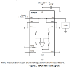
there are some problems with INA253-Q1 (100 mV/A module): i linked the 5 V power supply to VS and GND connectors, the current generator is linked to through a breadboard and a resistance of 10 Ω to the IS+ and IS- connectors with an output current of 0.18 A. Ref1 is connected to GND and ref2 is connected to VS. Without connecting ref1 and ref2 connectors, the output voltage is proportional to the current according to the datasheet. But, when I connect ref1 to ground it happens that power supply of the operational amplifier goes to short circuit. So, how is it possible that the sistem works without connecting both ref1 and ref2? According to the schematics in the datasheet, if the resistance between ref1 and ref2 is measured, but it isn't 100 kohms. Instead of that, I have 30 kohms. How is it possible? I attach the functional block diagram of the manual.

  • Hi,

    Just wanted to make sure – are you testing with the EVM or the chip directly? The reason I ask is because there are simple circuits on the EVM to configure the REF1/2.

    Regards, Guang  

  • Yes, I am testing with the EVM. Then, ref1 and ref2 are connected to any place or are they floating?

    Regards

  • Hi,

    That makes sense. On the EVM, REF1 is shorted to VS and REF2 to GND. They are not floating

    Regards, Guang  

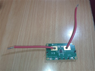
  • Thanks. Now 2 of 3 boards are working with the correct gain (200 mV/A and 400 mV/A), but the board with gain of 100 mV/A is not working properly giving a gain of 350 mV/A. This board has the difference, in comparison with other two, of having 2 wires soldered in T101 and T102 slots as shown in picture. What could be the reason of the problem?

    Regards

  • Hi,

    If you short the two wires together and tie to GND (or any fixed potential, such as VS), what do you measure at the output? Next when you pass a known current through the wires, measure the output again. Now do a differential calculation, which should yield the right gain.

    Varying the current and measure the output at a few data points should reveal if the part is behaving correctly.

    Regards, Guang  

  • Hi,

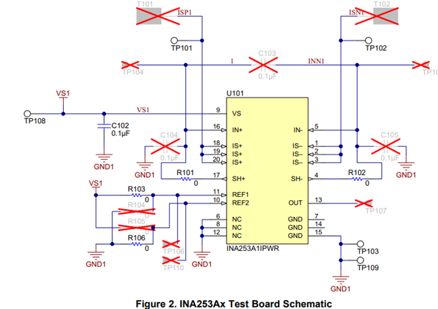
    when shorting the two wires to VS, I measure the voltage between OUT pin and GND pin on the right side of the board. I tested the board for some known values of the current, until the value of 1 A, and I did this differential calculation on the voltage in order to obtain a value in mV/A, but the problem persists and the results are not matching the value of 100 mV/A. I will attach the scheme of the circuit.

    Best regards.

  • Hi,

    Sounds good, it would also be helpful to tabulate the input/output measurements.

    Regards, Guang  

  • Dear Guang,


    Thanks a lot for your support. You have made me save a lot of time.


    FOR THE RECORD.

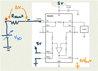
    I just want to remark that from the INA253EVM User’s Guide the following schematic is the first one for the demonstration board that the user finds. As you can see REF1 and REF2 are floating, that should be corrected by Texas Instruments because is confusing.

    The test.

    We have implemented in our laboratory the following test:

    The voltage supply VDD sweeps a range of voltages from 2.2 V to 11.4 V while Rload remains constant. For every value of VDD, the drop voltage across Rshunt is recorded together with the output voltage from the demonstration board INA253EVM.


    The problem.

    The INA253EVM comes with 3 samples with different gain: 100 mV/A, 200 mV/A and 400 mV/A. The tests carried out for boards with gains 200 mV/A and 400mV/A worked well. Experimentally, we found that these gains were correct. However, the measures for the board with 100 mV/A shows that the real gain is 350 mV/A which is weird.

    The only thing that we have done different in this board is to soldered a cable on the pads IS+ and IS-, could the overheat made vary any of the resistor of the internal differential amplifier? The thing that drops me mad is the exact value of 350 mV/A.


    Issues for my application.

    The INA253EVM under the configuration of REF1=5V and REF2=0V gives Vout=2.5V when there is not current through IS+ and IS-. The current that we want to measure will reach up to 15 A. That means that if the board with 200 mV/A is taken when 15A passed through the output would reach to 2.5+(15x0.2)=6V which is not possible because the INA voltage supply is 5V. In other words, only the board with a gain of 100mV/A works for us.

    Best regards.


  • Hi,

    Figure 1 is a block diagram of the device, while Fig 2 is the real schematic of the EVM itself. Sorry it confused you.

    It is a mystery to me also why the gain would be anything but 100mV/A, soldering a pair of cables should not change the gain. Is it possible to repeat the test in the same fashion as the others? Maybe something will turn up along the way.

    For your application, an alternative is to remove Rx03 and place it at Rx04 instead (please refer to Fig 2), then the quiescent output would be referenced to GND. This way you could use one of the higher gain options.  

    Regards, Guang