This thread has been locked.

If you have a related question, please click the "Ask a related question" button in the top right corner. The newly created question will be automatically linked to this question.

XTR111-2EVM: XTR111-2EVM

Part Number: XTR111-2EVM
Other Parts Discussed in Thread: XTR111, TIDA-01536

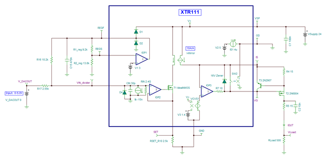
Hello everyone, I'm using the XTR111 to convert a 0-5V input voltage to a 4-20mA output, as shown in the picture below.

I would like to know in this case the transfer function for the output current.

Luigi

  • Hi Luigi,

    Attached is a simulation with a simplified TINA simulation for the XTR111 device.  Please note, the simulation below uses an idealized/approximate/simplified XTR111 circuit model, the XTR111 circuit attached is not an official model and therefore it does not simulate the XTR111 supply headroom limitations, AC/bandwidth, DC accuracy and noise performance of the XTR111. However, this ideal/simplified XTR111 simulation could be used as a tool to quickly verify the input/output ideal transfer function.

    - The XTR111 transfer function is as described in the datasheet:  Io = VIN / RSET* 10

    - Since the circuit requirement is +5V input voltage to provide +20mA output, RSET is set to 2kΩ to provide a 20mA output, for a +5V input

    - The XTR111 regulator is set to +5V.  The following equation sets the output voltage of the regulator:  VREGF = 3V * (R1 + R2) / R2. 

    Therefore, the output of the voltage regulator can be set to +5V by selecting R1 = 9.2kΩ and R2 = 13.8kΩ as shown on the circuit below.

    - Since you require an output current of 4mA output current when VDAC = 0V, a voltage divider with resistors R16 =10.2kΩ and R17 = 2.55kΩ is connected between REGF and VIN. This voltage divider produces an input voltage of 1V at VIN when VDAC = 0V.  This results on Iout = 4mA when VDAC =0V.

    - Below is the XTR111 simulated circuit and DC sweep simulation results for VIN = 0V to +5V producing Io = 4mA to 20mA. 

    TINA Simulation file:

    XTR111_forum_4-20mA_vin0-5V_Vin.TSC

    Thank you and Regards,

    Luis

  • Thank you Luis for your prompt response.

    In this case, do the tolerances of resistors R16 and R17 contribute to the TUE (Total Unadjusted Error)? Let me explain further. In the Design Guide of TIDA-01536, the total calculation of the XTR111's TUE is reported. I'm including the equation below for convenience.

    How does this equation change taking into account resistors R16 and R17 and the output components of the EVM(Mosfet, TVS, 15Ohm)? Moreover, should we also consider the voltage regulator error (REGF) in this equation?

    Looking forward to your kind response,

    Luigi

  • HI Luigi,

    The regulator of the XTR111 offers limited accuracy.  The regulator reference voltage offers a 3V nominal, 2.85V minimum and 3.15V maximum as shown on the XTR111 datasheet. Therefore, the variation on the 5V regulator voltage output will be dominated by the regulator voltage reference, and the regulator output range will be about +4.75V min to +5.25V max, or roughly ±5% initial accuracy error at room temperature, plus the drift associated with the regulator.

    Most applications using a DAC will configure the device to produce a 1V to 5V signal, to produce a 4mA to 20mA output. If the application allows to adjust the DAC voltage to a range of 1V to 5V, to produce 4mA to 20mA output, this will be the lowest cost solution reducing errors, and reducing complexity of the circuit.

    If the application does not allow to adjust the DAC voltage to 1V-5V range, then another option is to use an external precision reference and a precision voltage divider circuit to produce the 1V input.  Precision references such as the REF35xxx, REF20xx (and many others) offer initial accuracy at ±0.05%.  A resistive divider built with ±0.05% tolerance resistors will produce a very worst case error of 0.1%, nevertheless, the typical error will be typically much lower, depending on the resistor tolerance distribution. You can add the estimated errors of the voltage divider, and reference accuracy on the root-sum-of -square equation above.

    The 15Ω series resistor at the source of the FET, and the 15Ω series resistor at the drain of the FET do not add an error in the output current of the XTR111. However, the designer needs to ensure to allow the proper compliance voltage, in other words, the XTR111 supply has to be high enough to allow the circuitry enough headroom to operate in the linear range. The XTR111 requires more than 2V headroom below the voltage supply to operate.  You also need to account for all the voltage drops on the series resistances on the output current path, the required external FET transistor VSD voltage drop, and the 2V compliance required for the XTR111 operation. 

    For example, if the device is powered with a +24V supply, and require to source 20mA output current, the max voltage supported at the load output will be around ~21V when accounting for all the I*R series resistance voltage drops, XTR111 2V compliance voltage, and the FET transistor VSD voltage.  Here is a circuit diagram showing the voltage drops across the series resistance:


    The TVS diodes and protection diodes will have some small leakage currents, but do not directly alter the transfer function.  For example, some TVS diodes specify a leakage current of ~1µA when operated at voltages below the standoff voltage, which is small compared to your 20mA output current.  

    Thank you and Regards,

    Luis