This thread has been locked.

If you have a related question, please click the "Ask a related question" button in the top right corner. The newly created question will be automatically linked to this question.

LMP8601-Q1: Maximum Input resistance allowed at IN+ & IN- Inputs

Part Number: LMP8601-Q1
Other Parts Discussed in Thread: LMP8601, LMP8602-Q1, INA185, LMP8602

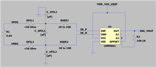
We are monitoring the current through a Shunt resistance of 40mOhm through LMP8601-Q1 with an GAIN configuration of ~50V/V.

For the diagnostic purpose, we would like to inject some voltage at IN+ & IN- pins with a voltage difference for which following circuit modules would response.

To do so, we really need the resistance ("RSER1 & RSER2")  at the IN+ & IN- pins in the range of 1K ohm to 10K ohm.

So now the questions are,

1. Is it allowed to have 1K ohm to 10K ohm resistance in front of IN+ & IN- pins of LMP8601-Q1 device?

2. What is the functional impact of having high input resistance in front of IN+ & IN- pins of LMP8601-Q1 device?

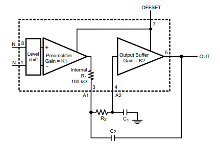
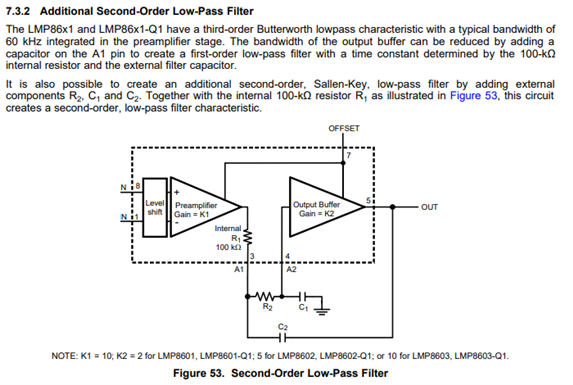
Refer the LMP8601-Q1 input path proposal in the figure below:

  • Hello,

    1. Is it allowed to have 1K ohm to 10K ohm resistance in front of IN+ & IN- pins of LMP8601-Q1 device?

    Having large resistors in front of the input stage of our current sense amplifiers is not recommended because the resistors will change the gain and offset of the system. This is caused by the bias current flowing into the INP and INN pins, as is described in this video: https://www.ti.com/video/6319688089112  as well as this video: https://www.ti.com/video/6219017476001.

    If all you need to do with the input structure is filter the input signal you could consider using the device's built in filter capabilities (described on pages 20-22 of the datasheet).

    If you wish to add resistors to the input pins of the device we generally recommend the total resistance between the shunt and the inputs be less than 10 ohms in value.

    Let me know if you have any more questions,

    Levi DeVries

  • Hi,

    Thanks for your response.

    Is there any way to estimate the difference at the output voltage due to impact on device gain and offset voltage due to high resistance at the input path?

    From the LtSpice Simulation I have not observed a major difference in the LMP8601 VOUT when 2K is used at the input of LMP8601.

    Simulation - Circuit configurations:

    • Current measured is 0.4A & 1A.
    • Shunt resistor used is 40mOhm.
    • Gain increased to 49.4V/V using an external resistor option. (i.e., A1 pin with A2 pin are connected together with VOUT pin through an external 168.1K Ohm resistor)
    • Two set of simulations performed at following two configurations.
      • With 0.05 ohm in series
      • With 2K ohm in series 

    Simulation - Results:

    CONDITION I_FIRE (A) VDIFF (V) VOUT (V) Gain_calculated Gain_set
    30 Ohm in series 0.4 0.016 3.377 54.81 49.37
    30 Ohm in series 1 0.040 4.561 51.53 49.37
    2K Ohm in series 0.4 0.016 3.368 54.63 49.37
    2K Ohm in series 1 0.040 4.545 51.51 49.37

    Queries to be clarified:

    1. Could you please explain why there was no major change at the VOUT (V) when 30 Ohm & 2K ohm resistor used in series (In simulation)?
    2. Even if the circuit working fine with 2K Ohm resistor in series in simulation, do we have a possibility of risk that the actual device won't work in the actual board?
    3. I have connected LMP8601 device A1 pin with A2 pin then connected together with VOUT pin through an external 168.1K Ohm resistor to increase the device gain to 49.37V/V. But as per the simulation results the gain is observed as mentioned in the table above. What factors could cause the device gain to vary than the set limit?
    4. What is the suitable filtering scheme (i.e., at the A1 and A2 pin) for the increased gain circuit configurations?
  • Hello,

    We again do not recommend putting any resistance before the inputs of this device due to the reduced performance it may result in.

    Could you please explain why there was no major change at the VOUT (V) when 30 Ohm & 2K ohm resistor used in series (In simulation)?

    As the second video I posted explains, many of our current amplifier models do not capture the full behavior of the part, so that is probably what is happening here. I would need to check with our modeling expert to understand the full capabilities of the model.

    Is there any way to estimate the difference at the output voltage due to impact on device gain and offset voltage due to high resistance at the input path

    The best way is to make a simulation for the input structure. The video I linked to above is key for understanding these issues: https://www.ti.com/video/6219017476001?keyMatch=INPUT%20FILTER%20ERROR 

    You can also consult the datasheet plots for the input bias current to understand what currents the device will draw from the circuit: 

    I have connected LMP8601 device A1 pin with A2 pin then connected together with VOUT pin through an external 168.1K Ohm resistor to increase the device gain to 49.37V/V. But as per the simulation results the gain is observed as mentioned in the table above. What factors could cause the device gain to vary than the set limit?

    The results you posted seem to indicate an offset error rather than a gain error. Based on the numbers you have here, it looks like there is about 1.75mV of offset error referred to the input. It is hard to say exactly where this is coming from without knowing more about the voltages you are applying to the device. 

    You are probably measuring the voltage across R1, but if you measure the voltage directly at the device pins you will probably find that the gain is closer to what you expect.

    What is the suitable filtering scheme (i.e., at the A1 and A2 pin) for the increased gain circuit configurations?

    You could consider switching to the LMP8602-Q1, which is a 50 V/V part so you would not need any additional gain and can use the A1 and A2 pins with the Sallen-key filter design posted above. This will also allow you to avoid the issues inherent in using a filter by the input pins.

    Let me know if you have any more questions,

    Levi DeVries

  • Hi,

    Thanks for the detailed explanation.

    As mentioned in the video "https://www.ti.com/video/series/precision-labs/ti-precision-labs-current-sense-amplifiers.html",I am calculating the adjusted new offset voltage and new gain value due to the use of filter resistor.

    • For the estimation of new input offset voltage due to the use of filter resistor at input, following formula has been used. In this formula, Ios parameter needs to be calculated as difference between the input bias current at both inputs i.e., IB versus Vdiff needs to be evaluated from the datasheet waveform. But this information is not available in the LMP8301-Q1 datasheet (as given for INAx series devices). 
      • Please provide the IB versus Vdiff (at LMPx inputs) information to evaluate the Ios parameter for the calculation.


    • For the estimation of new gain value, due to the use of filter resistor at input, following formula has been used. In this formula, RINT or RFB value needs to be used for the calculation of impact on gain value. But these resistor values are not available in the LMP8301-Q1 datasheet (as given for INAx series devices). 
      • Please provide the RINT or RFB values to evaluate the new gain value due to the use of external filter resistor.

  • Hello,

    Did you check my suggestion about using the 50V/V part for your use case? This would be a more appropriate way to use the device.

    Please provide the IB versus Vdiff (at LMPx inputs) information to evaluate the Ios parameter for the calculation.
    Please provide the RINT or RFB values to evaluate the new gain value due to the use of external filter resistor.

    I will need to check on this and get back to you next week for these values.

    Thanks,

    Levi DeVries

  • Additionally,

    For the estimation of new gain value, due to the use of filter resistor at input, following formula has been used. In this formula, RINT or RFB value needs to be used for the calculation of impact on gain value. But these resistor values are not available in the LMP8301-Q1 datasheet (as given for INAx series devices). 

    This formula is useful for the INA185, but is is not applicable for the LMP8301-Q1 and is not found in the LMP8301-Q1's datasheet. For the LMP830-Q1, the only method mentioned in the video that will work to predict the new gain values is simulation.

    Levi DeVries

  • Hi, 

    Exactly this also a concern for me. Since I have raised a query for the LMPxx series but in the suggested video material INAxx series has been considered as an example.

    So, I felt INAxx and LMPxx series have a similar method to estimate the change in offset and gain due to the use of input filter circuit. Also, nowhere it has been mentioned in the video that this is applicable only for INAxx series.

    Hence, I thought to clarify my understanding here and now it is confirmed that the approach suggested in the video will not be suitable for LMPxx and only simulation is an available option to validate the impact on offset voltage and gain.

    Now this requires a clarification about the following points related to the simulation. They are,

    1. As mentioned by you in the previous conversation reply (Refer snapshot below) that "many of our current amplifier models do not capture the full behavior of the part, so that is probably what is happening here. I would need to check with our modeling expert to understand the full capabilities of the model". 

    Since we have an only option to verify the impact is simulation, how confident we can rely on the simulation and model?

    2.Do we have any difference between the simulation models of LMPxx series Pspice model (downloaded from TI site) and inbuilt model available in TINA? 

    3. Also to do the simulation I need the details requested in the previous conversation (Refer snapshot below).

  • Hi,

    Is there any update on this request?

  • Hello,

    Sorry for my late response, I am still waiting to hear back from our modeling expert on your specific questions.

    Thanks,

    Levi DeVries

  • Hello,

    I was able to check with our modelling expert and unfortunately as this is an older product we don't have much information on what the model is capable of in terms of the input structure. This model may be inadequate for the advanced cases you are trying to simulate with this model. Many of our models contain information in the macro detailing what parameters of the part are captured in the model but this model does not have this information.

    I spoke to some of the designers and they recommended that you limit to the input resistance to less than 1% of the input resistance, or 2.9K. You will still have some gain degradation in this range and unfortunately we have no formula to determine this degradation. Outside of the ±1% of the input resistance the part's behavior becomes more unpredictable as the input structure is used in an irregular mode.

    As an alternative solution, you should use the LMP8602, which has a gain of 50V/V, exactly your target gain, and remove the high resistance filter on the inputs of the device. If a filter is needed for your system, you should use one of the filter designs specified in the datasheet on pages 20-22 and should not put a large filter on the inputs of the device.

    Let me know if you have any more questions,

    Levi DeVries