LM3488: PSPICE result discussion to generate +/-80V

Part Number: LM3488
Other Parts Discussed in Thread: TIDA-010057, LM5155

Tool/software:

Hello,

We are designing one own Medical product in which we need +/-80V and from Ultrasound application, we found it with LM3488.

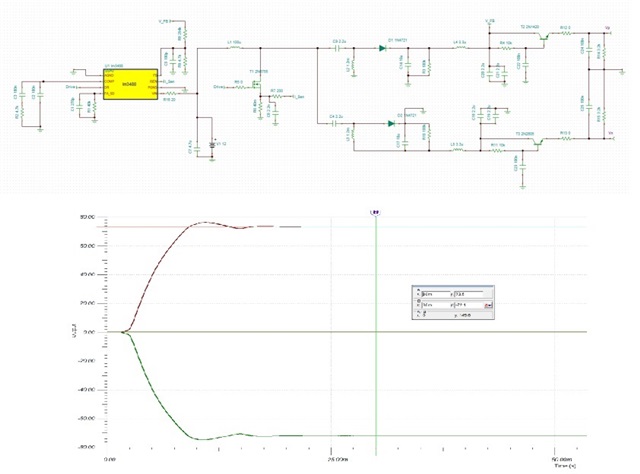
Based on the application circuit, we prepare the PSPICE in TINA and below are the results,

Title: Clarification Needed on LM3488 Simulation Results and Load Behavior

Introduction: I recently conducted a simulation on TINA using the LM3488 for a project and encountered some unexpected results. I would like to seek guidance from TI experts on the forum regarding the interpretation of these results and potential troubleshooting steps.

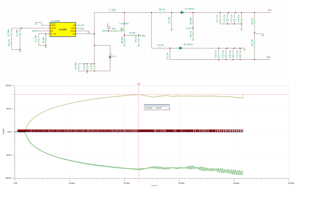
Simulation Overview: The objective of the simulation was to evaluate the performance of the LM3488 in a specific configuration. The expected output range was from -80V to +80V at 25mA. Reference stimulation circuit for LM3488 was taken from TIDA-010057 document.

Results: Two observed results are been shared below:

  1. Without load

Output Plot Analysis:

  1. Green Line:Represents Vp=+80VV_p = +80VVp​=+80V
  2. Red Line:Represents Vn=−80VV_n = -80VVn​=−80V
  3. Brown Line: Represents Mosfet switching

Result:

We got the desire result of -80V to +80V for which the image(1) is attached below.

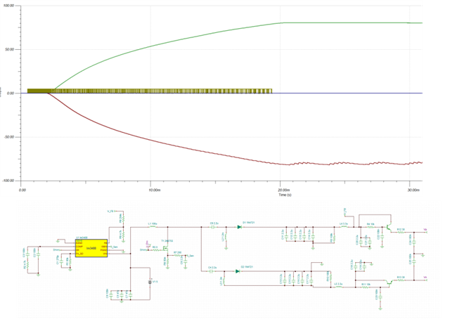
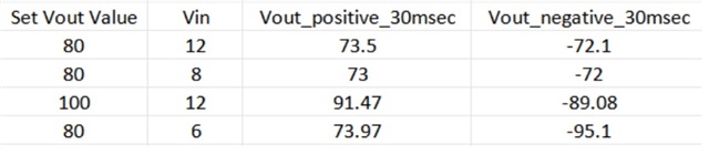
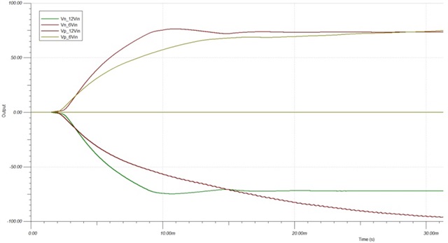
  1. With loadto draw 25mA

Output Plot Analysis:

  1. Green Line:Represents Vp=+80VV_p = +80VVp​=+80V
  2. Red Line:Represents Vn=−80VV_n = -80VVn​=−80V
  3. Brown Line: Represents Mosfet switching

Result:

On adding load we didn’t got the expected result instead we observed that negative voltage reaches 80V and above whereas positive voltage never reaches 80V and is fluctuating. Image(2) is attached for your reference.


Questions:

  1. Voltage Drop with Load:
    1. Why are we observing voltage fluctuation on positive voltage rail ?
  2. Circuit Stability:
    1. Considering the expected output range and the observed performance, what measures can be taken to enhance the stability and reliability of the output voltage?
  3. Component Selection:
    1. Are there specific components, particularly the Mosfet, that could be causing the observed discrepancies? If so, what alternatives would you recommendform TI library to be used?
  4. Simulation Accuracy:
    1. How accurate are these simulation results likely to be compared to real-world testing? What factors should be accounted for to align the simulation closely with practical implementation?
  5. Further Optimization:
    1. What additional steps or modifications could be made to the circuit to ensure it maintains the desired output range under varying load conditions?

Conclusion: Any insights or suggestions from TI/forum members with experience in using the LM3488 or similar simulations would be greatly appreciated. I am particularly interested in understanding the root cause of the voltage drop and how to mitigate it effectively.

Thank you in advance for your assistance.

Please find the attached simulation files.

Regards,

Alpesh

lm3488_full_Working (1).zip

  • Hi Alpesh,

    Thanks for using the e2e forum and attaching the sim files.
    Looking at the schematic, I saw that you used different inductances at primary and secondary sides. This will not work for a SEPIC design.
    In SEPIC topology, primary and secondary side inductor need to have the same winding ratio to work properly.

    When boosting from 5V to 80V, it makes sense to adjust winding ratios to achieve a lower duty cycle, but then a flyback topology needs to be used.
    You can use the LM3488 as Flyback controller as well, so I strongly recommend to change the topology.

    Regarding your questions:
    1./2. I would assume this is the result of using a SEPIC topology with different winding ratios. This also leads to instability of the circuit
    3. The inductors should be the root cause for this behavior. The FET should not be the problem here.
    4. The simulation model is a simplified version of the physical device. Features like UVLO, overcurrent protection and generation of the PWM control signal are simulated just like the real device would behave, but there is no simulation of device variances, temperature or noise related behavior.
    5. I recommend using the Power Stage Designer tool to find suitable transformer components, calculate current ratings and duty cycle and double check the compensation network. The tool can be found here:
    https://www.ti.com/tool/POWERSTAGE-DESIGNER

    Best regards,
    Niklas

  • Hello Niklas,

    Thanks for the details,

    Regarding your suggestions:

    1. /2. I would assume this is the result of using a SEPIC topology with different winding ratios. This also leads to instability of the circuit

    Ans:) Primary and Sencondary side inductor values are been taken from TIDA-010057 document. For Reference: https://www.ti.com/lit/an/sloa284a/sloa284a.pdf?ts=1719809832300&ref_url=https%253A%252F%252Fwww.google.com%252F

    1. The inductors should be the root cause for this behavior. The FET should not be the problem here.

    Ans:) What should be the value as per your recommendation. We tried stimulating with 2 inductor sharing same core having same value for Positive and negative filter I.e replacing 1mH.

    1. The simulation model is a simplified version of the physical device. Features like UVLO, overcurrent protection and generation of the PWM control signal are simulated just like the real device would behave, but there is no simulation of device variances, temperature or noise related behavior.

    Ans:) Ok we got that. But in TINA stimulation we observed something I.e operating at 12V input voltage at 25mA output current we got +73.5V and -72.1V which was very near to TI document results. The result plot is attached for your reference.

    1. I recommend using the Power Stage Designer tool to find suitable transformer components, calculate current ratings and duty cycle and double check the compensation network.

    Ans:) This software will give values for Single output but we want dual supply I.e +ve and _ve. What are the things that we should be keeping in mind to get the required result. We also performed stimulation by changing input voltage as well as setting up output voltage here are the results.

    Question:- Is there any limitation of Input voltage to generate the +/-80V@25mA in any simulation model OR actual circuit? Is this any minimum input voltage/current required to get +/-80V@25mA as we get the output from 8VIN to 12VIN and lessthan 8V it is distorted in simulation?

    We observed that at Vin voltage less then 8V we get the distorted output result and negative voltage surpass -90V (don’t know why ) but at 12V we got the required result.

    Combine result of 12Vin and 6Vin rest all the circuit remains same.

    Question : - If we use the same schematic, including BOM and layout from the TIDA-010057 to generate +/-80V@25mA from 5.5V DC, Are we able to get the result in actual board?

    Question : Can you please guide us how to generate +/-80V@25mA from 5.5VIN?

    Regards,

    Alpesh

  • Hi Alpesh,

    Thank you very much for the detailed response.
    I was not aware that this is based on a TIDA design.

    This is a build and tested board, so I would not assume that the inductor choice is a design error then. The waveforms within the TIDA report also confirm that this design runs stable.
    After requesting some internal feedback on this TIDA design, it turns out that the inductors are not coupled, so this approach is indeed feasible.

    As this is a validated design, the error must come from the simulation and my comment on questioning the topology was wrong.
    I am sorry for causing confusion on this.

    I know that we also have a PSpice simulation model available for LM3488.
    For cross checking, I will set up the same schematic in PSpice and check if the design works better or shows the same behavior.
    This will show if there might be a problem with the LM3488 TINA model itself.

    I will update you within 1-2 days on my findings.
    Best regards,
    Niklas

  • Hello Niklas,

    Is there any update for us on simulation results?

    Regards,

    Alpesh

  • Hi Alpesh,

    Thank you very much for your patience.
    I have run simulations in both TINA and PSpice, and also checked for similar requests from the past, but all of that without success.

    The same request has already been posted over two year ago for the PSpice model. Here similar issues where seen of Vout not reaching the target, but it is unclear if this customer was successful in the end.
    https://e2e.ti.com/support/power-management-group/power-management/f/power-management-forum/1089164/lm3488-problem-for-pspice-for-ti-simulation-based-on-tida-010057

    I still cannot say if the problem comes from the LM3488 model itself, or if this can be fixed through external circuits.
    I can review the LM3488 model and check if there are parts that may differ from the physical behavior which leads to the simulation inconsistency, but this process will take me several weeks.

    The TIDA board is not available for order in the TI shop, but if verification of this SEPIC design on a physical board is desired, you may get in contact with your local TI sales or field application representative, so we can initialize a sample delivery of this TIDA-010057 board.

    I am very sorry for the inconvenience this simulation model has been causing so far.

    Best regards,
    Niklas

  • Hello Niklas,

    Thank you very much for your efforts to support us.

    I am trying to search the TI FAE for the Gujarat, India and if you have then please share so I can ask him for the TIDA-010057 sample for the development.

    Regards,

    Alpesh

  • Hi Alpesh,

    Thanks for the feedback.
    Unfortunately, I do not have the contact information for our offices in India, but you can always contact the TI support center and get forwarded from there.
    https://www.ti.com/info/contact-us.html

    Thanks and best regards,
    Niklas

  • Hello Niklas,

    Thank you very muck for your support.

    Regards,

    Alpesh

  • Hello Niklas,

    I have contacted the TI FAE from India and send email as well as talk with them on call.

    TI FAE says that he is not supporting on this If you want to be sure then you need to make your own board if it is not available from TI store.

    Is it so?

    How can I be sure about the required result with the circuit to be used in the refeence design as the result is different in simulation from TINA?

    Is there any way because instead of spending time and money in designing the circuit If I get from TI then it is better for me to test and confirm the result then I will make my own design for proto board with required our own hardware.

    I hope you can understand and provide the better way on this.

    Regards,

    Alpesh.

  • Hi Alpesh,

    I can fully understand that this puts you in a difficult situation.

    As of right now, I cannot say how usable the results of the TINA simulation model are. Because of this, I would avoid taking this simulation results as reference.
    If the TIDA board cannot be sampled, there is no cheap/fast way of validating this design with LM3488.

    An alternative solution would be changing to a different device for this application.
    LM5155 is a more modern device than LM3488, with improved features and even better pricing. We have a lot more documentation resources for this device, including newer simulation models, quickstart calculators and several EVM boards that can be ordered from the TI shop.

    I would recommend to validate this design by using the LM5155 controller.
    More details can be found on the product page: https://www.ti.com/product/LM5155

    Best regards,
    Niklas