This thread has been locked.
If you have a related question, please click the "Ask a related question" button in the top right corner. The newly created question will be automatically linked to this question.
Tool/software:
Hello,
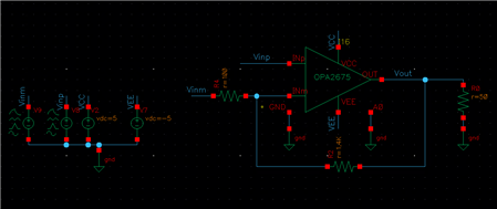
I am using the unencrypted Pspice model for the OPA2675 in a Cadence Virtuoso testbench. I am trying to drive the gates of two FETs with their own respective op amp, and I like the OPA2675 for its fast slew rate and high output current. During simulation, I noticed the slew rate of the OPA2675 is less than what I anticipate. Below is a screenshot of a separate testbench I am using to characterize the OPA2675:
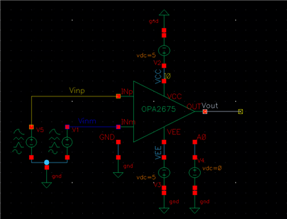
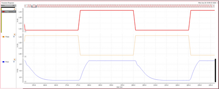
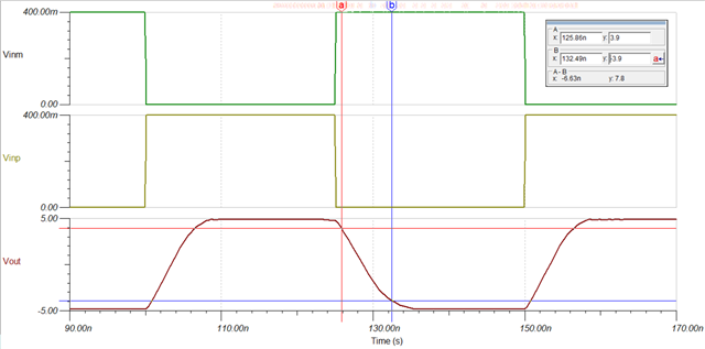
I am applying an ideal differential signal to the input terminals, and the rails are biased at ±5V. Below is a screenshot of the transient sim results for this testbench:
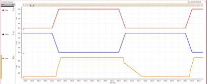
The rising edge of the op amp's output seems on par with the datasheet, but the falling edge is degraded. Can someone please explain why I am getting this result?
Thank you for your help!
Braden
Hi Braden,
Could you give me some more information about how you're using this? What is your target gain-I don't see any feedback in your screenshot.
Thank you,
Hypatia
Hello Hypatia,
Thank you for your reply. I am using these op amps to drive the gates of a >100 MHz CMOS circuit. I am trying to heavily saturate the MOSFETs in a short amount of time. I initially went for this open loop setup, because I want to drive the op amp to its rails. My differential signal has a Vpp of 400mV, so I require a gain of 12.5 to saturate the op amp. After implementing a feedback network in my design, I find a similar result:
I would like to acknowledge, I do not know a lot about feedback networks for differential signals; I am more familiar with feedback networks for single-ended signals. So if there is a better feedback design for this circuit, please let me know!
Thank you,
Braden
Hey Braden,
I did some testing in simulation, and I agree that the slew rate is too low. I think a big part of that, especially the extremely slow falling rate, is unfortunately due to inaccuracy of our model.
However there were a couple things I wanted to note about the part that may have an effect:
Since the bandwidth of current feedback amps is dependent on Rf and gain, we can estimate from the datasheet that a Rf of 1.4kΩ in a gain of 12.5 will give you a BW around 30MHz. It looks like your input is 20MHz right now, so you might see some bad effects from that, especially outside of simulation. If you are able to change the feedback, I would suggest a Rf = 400Ω and Rg = 32, which would give you a BW of 100MHz. If you need that high of Rf and input frequency, I would have to suggest a higher bandwidth part.
I also noticed that the problem of slow fall time was more pronounced when the input had a higher DC value. Below is a sim I tried where the input is centered around 200mV instead of the 1.2V in your simulation. The falling time is still a bit slower than rising (1ns slower), but it is less pronounced. I wonder if maybe it's saturating too hard at the positive rail when biased higher?
I don't know much about your application, so I don't know if it would be possible to do that, but I thought it was interesting. It could just be a simulation oddity also.
I also wanted to mention that I don't suggest using the amplifier in an open loop configuration, as we don't characterize the part for that and most of the datasheet information would not apply.
Again, I believe what you're seeing is problems with the slew rate modelling of the part. I would definitely trust the datasheet spec over the sim.
Please let me know if you have any further problems or questions!
From,
Hypatia