TLV9062: Design suggestion for Precision Rectifier Circuit for CT Signal Conditioning

Part Number: TLV9062
Other Parts Discussed in Thread: INA351

Tool/software:

Hi E2E

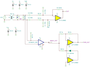
I am using TLV9056 as a differential amplifier to amplify the output from the current transformer (1:1000)  of input frequency of 50Hz, this is to measure the line currents and the noninverting pin is biased with 3.3V. 

Below is the reference schematic for that 

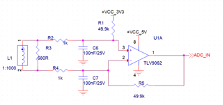
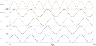
and the above circuit is working as expected as per design.


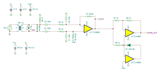
I also want to repurpose the same CT output for some different applications for which I need to convert the same CT output into pulsating DC, I am referring to TI Application note sboa296 , I need design suggestions on how can I use the same CT output for two different circuits which are having two different biasing.

So conclude my requirements, I want to use the CT output for two applications

1. Differential amplifier biasing with 3.3V voltage 

2. Pulsating DC output from CT with a certain gain.

Please let me know if you need any other information.

Regards

Chaitanya 


  • Hi Chaitanya,

    Do you want the full wave rectifier circuit to be centered at 0V as what is show in the application note? 

    Best Regards, 

    Robert Clifton 

  • Hi Robert 

    Yes, I want the output of the full wave rectifier to be centered at 0V.

    BR

    Chaitanya 

  • Hi Chaitanya,

    The common mode voltage was the primary problem that I faced when trying to merge these two circuits together. But I think I have something figured out. 

    You'll notice that I had to add two more supply voltages to your system. a 2.5V and -2.5V that power the INA351. This is to ensure that we don't distort the signal when it goes below 0V, that way, there's no distortion seen when it goes through the full-wave rectifier. 

    You can also see I added some DC blocking capacitors (C4 and C5) to the system to separate the biasing voltage. Also R9 was added only for spice simulations as I needed a DC bias point to not break the simulation. 

    See the results below: 

    If more gain is needed in the system going to the full wave rectifier, then a different instrumentation amplifier with higher gain would be needed, or another amplifier gain stage. 

    Let me know what you think of this proposal. I'm sure there are alternatives to this option. 

    Best Regards,

    Robert Clifton 

  • Hi Robert 

    Thanks for your suggestion, I can use this proposal as a base and build on it. I wonder in case if I want to use the output from U1 and consider the center value for the full bridge as the Vref value, Do you suggest some design recommendations or application notes that I can refer to for that?

    BR

    Chaitanya 

  • Hi Chaitanya,

    I don't believe that we have a piece of content that details what you are looking for. 

    Are you saying using the U1's output to be the center value of the full bridge rather than 0V is also an acceptable design? 

    Best Regards,

    Robert Clifton 

  • Hi Robert 

    I am trying to optimize the design and exploring the other possible ways for my use case.

    Yes, you are correct, one option that I can look for is, using the output of  U1 and the Vref as the central value of the full bridge.

    BR

    Chaitanya 

  • Hi Robert

    Do let me know if you need any more details.

    BR

    Chaitanya 

  • Hi Chaitanya,

    Sorry for the delay. As you can see from the results below, the full wave rectifier won't come out as cleanly when rectifying it with a 3.3V offset but it still works. I also had to add a 3.3V supplies to the noninverting input of U3. 

    R9 was added only to help the spice simulation. It's not needed in the actual design. 

    I've also attached the spice simulation so you can also experiment with the circuit.

    TLV9062 Design suggestion for Precision Rectifier Circuit for CT Signal Conditioning.TSC

    Best Regards,

    Robert Clifton