This thread has been locked.

If you have a related question, please click the "Ask a related question" button in the top right corner. The newly created question will be automatically linked to this question.

PGA308: Differential Input Voltage Range

Part Number: PGA308

Tool/software:

Good morning Support Team,

I found the following stated on the datasheet:

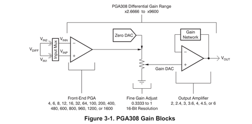
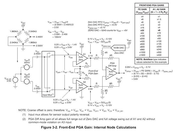
Linear input range is the allowed min/max voltage on the VIN1 and VIN2 pins for the front-end PGA to continue to operate in a linear
region. The allowed common-mode and differential voltage depends on gain and offset settings. Refer to the PGA308 User's Guide
(SBOU069), for more information.

However, I'm unable to locate the allowed differential input voltage range permitted in the User Guide.

I have an application that requires indirect output from the PGA308 (i.e. increased output with decreased input differential voltage & vice-versa) which I could do using a difference amplifier at the output of PGA308 but I don't want to if this can be achieved using the mux bit to ensure negative differential input voltage.

Will you please explain how to find out the rated differential input voltage range for the PGA308 & if what my application requires can be achieved by the PGA308 alone?

Thanks...

  • Hello Robert,

    The PGA308 is an instrumentation amplifier with programmable gain and programmable offset calibration.  Therefore, the maximum differential voltage is a function of the input common-mode voltage, the PGA308 gain settings, the PGA308 offset calibration settings and voltage supplies.

    The amplifier front-end offers programmable gains of x4 x6 x8 x12 x16 x32 x64 x100 x200 x400 x600 x800 x960 x1200 x1600; and the output stage amplifier offers gains: of 2x, 2.4x, 3x, 3.6x, 4x, 4.5x, 6x.  The device offers a fine gain resolution adjustment using a DAC.  The device also offers offset calibration adjustment.

    See figure 3-1:

    As with any instrumentation amplifier, there are limitations on the output voltage swing and input common-mode voltage range of the internal amplifiers. The block diagram on Figure 3-2 is represents the Front-End PGA within the PGA308. The equations provided on the block diagram, can be used to evaluate critical internal node voltages to ensure that output voltage swing and common-mode limits are not violated. Please note, it is possible to violate the limits of these internal nodes and continue to have apparently valid output voltages at VOUT of the PGA308.

    Therefore, the maximum allowed differential voltage is a function of the gain programmed into the PGA308 device, offset calibration, gain calibration, as well as the supply voltage, and the input common-mode voltage of the signal at the inputs of the device.

    The PGA308EVM software offers a "Block Diagram"  tab that allows you to manipulate the supply, offset and gain settings, and a "Simulation" tab that can then used to calculate the valid differential range of the PGA308 as a function of input common-mode for a given programmed gain settings and supplies.  All the supply, gain and offset gain settings are set on the "Block Diagram"; and then you use the "Simulation" tab to determine the max differential input range for a gain setting.   The blue circles on the "simulation" tab will be highlighted in red when one of the internal amplifiers is outside of output swing range when the input differential is too large for a given gain condition.  See below.

    Example when a violation has occurred:

    On the typical bridge conditioner application, the PGA308EVM calibration algorithm selects the best gain and offset calibration settings for a sensor zero-scale and full-scale voltage, for a given/desired minimum and maximum output voltage target range. 

    You may download the PGA308EVM software in this link.

    SBOC257  PGA308EVM Software

    https://www.ti.com/tool/download/SBOC257

    Thank you and Regards,

    Luis


  • Hi Luis,

    Thank you for the overview and response.  Is there a closed form expression to determine the valid range for the differential input voltage?

    Regards,

    Rob

  • HI Rob,

    I don't believe there is an existing tool to directly provide the max input differential voltage for the given settings in a closed form expression; and the User Guide does not provide a closed form expression, although an approximation may be derived using the equations of the block diagram of Figure 3-2

    In the typical application, the PGA308 is calibrated together with the bridge sensor to provide accurate results correcting for the sensor offset and instrumentation amplifier offset and gain errors.  The PGA308EVM software, during the calibration process, uses an iterative algorithm to find the optimal gain and offset calibration settings for a bridge sensor zero-scale and full-scale settings; for a desired minimum output and maximum output voltage requirement. 

    Because there is some variation in the offset (and gain error) inherent to the sensor, and variation on the intrinsic offset and gain errors of the instrumentation amplifier, the device relies on the calibration measurement, and relies on the fine offset and fine calibration gain adjustment to provide accurate results.

    Thank you and Regards,

    Luis 

  • Got it!  thank you for the help.

  • HI Robert,

    Many Thanks,

    Kind Regards,

    Luis