This thread has been locked.

If you have a related question, please click the "Ask a related question" button in the top right corner. The newly created question will be automatically linked to this question.

THS4541: Please recommend a suitable Fully differential amplifier.

Part Number: THS4541
Other Parts Discussed in Thread: AMC1300, ADC3662

Tool/software:

Hello?

There is a problem with the circuit currently being applied, so I would like to receive a recommendation for a suitable alternative method.

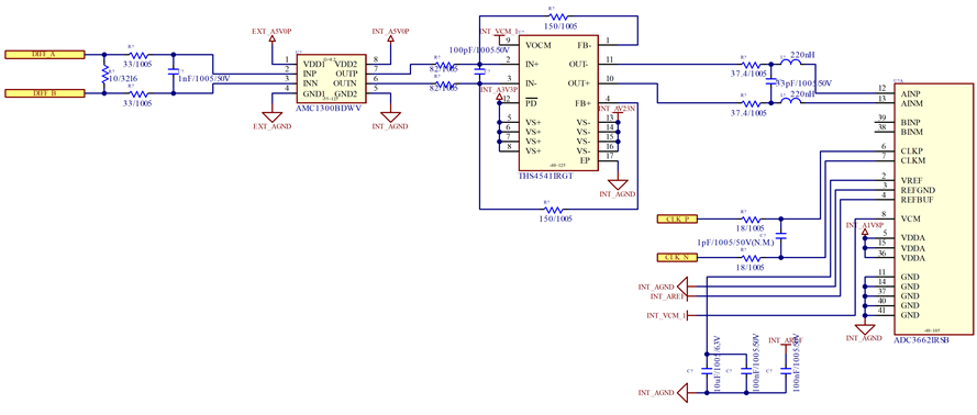
t receives the current current input, electrically isolates it, and then connects to the high-speed ADC in the following order: AMC1300BDWV -> THS4541IRGT -> ADC3662IRSB.
(THS4541 is a fully differential amplifier found in the ADC36 EVM.)

A burnout occurred during operation, so the design was reexamined, and it was discovered that the problem was that the input range of the THS4541 was 1 V differential.
- AMC1300 output is ±2 V, THS4541 input is ±1 V
- THS4541 output is R2/R1, ADC3662 input is differential 3.2 Vpp

Therefore, a 0.5 gain circuit must be added or the element must be changed, but space is an issue, so I would like to receive a recommendation for a suitable product.

(As a final method, I'm also considering changing the gain of the first input.)

Thank you for reading.

S.Y.Lee

  • Hi,

    Could you share a schematic for this portion of the circuit. Depending on the supplies and FDA gain, a 4Vpp input signal should not result in damage to the device. 

    Best Regards,

    Ignacio

  • Attach a drawing as shown.
    The FDA's gain is at the level of 1.82926, and if there is no other alternative and the input section is halved (input gain x 0.5), it will need to be changed to 3.65853.
    Before that, the FDA is reviewing other alternatives that may be appropriate.

    S.Y.Lee

  • Hi,

    Could you please confirm what supplies are connected to the FDA as well as the Vocm voltage. Also to get some clarity is the THS4541 getting damaged or does the device simply saturate?

    Best regards,

    Ignacio

  • VOCM of THS4541 is connected to VCM of ADC3662. it is 0.95 V.

    This is the same part as the EVM. (ADC364xEVM_RevF(004)_Sch_2022-04-01.pdf)

    When wired as is the current circuit, when 20 mA flows, the output saturates at 2.6 V. (except ADC3662, VOCM is floated)
    R (10 Ω): 0.02*10 = 0.2 V
    AMC1300 (G=8.2): 0.2 * 8.2 = 1.64 V
    THS4541 (G=150/82): 1.64 * (150 / 82) = 3 V (but it never exceeded 2.6 V, perhaps because it exceeded the input limit)

    But my question is not whether the current circuit works, but rather finding a replacement product since the input range of the circuit has been determined to be inadequate. (capable of 2 Vpp input and 3 Vpp output)

    S.Y.Lee

  • Hi,

    I believe the device is running into an output limitation not so much an input common-mode limitation. Could the customer measure the individual output pin when the input signal is present. If this is the case which it is pointing towards that, finding a replacement would not be useful as this device is already rail to rail out. The only way would be adjusting the supplies by having a more negative supply voltage.

    Best Regards,

    Ignacio

  • Hello.

    As confirmed after the previous answer, it has been confirmed that 3 V can be output by adjusting the resistance. (Output R.R is confirmed)

    When wired as is the current circuit, when 20 mA flows, (@ res: 10 -> 5 Ω, R1: 150 -> 300, except ADC3662, VOCM is floated)
    R (10//10 Ω): 0.02*5 = 0.1 V
    AMC1300 (G=8.2): 0.1 * 8.2 = 0.82 V
    THS4541 (G=300/82): 0.82 * (300 / 82) = 3 V

    So, I don't think the output itself is limited, and even if I use an amplifier that includes an additional negative voltage, I have confirmed the problem that due to the nature of the ADC3662 product, I have to change it back to positive voltage to receive input. (AINP/M, BINP/M of ADC3662: -0.3~2.1 V.)

    Accordingly, if VCM is set to 0.95 V, even if it is increased, the maximum input range of ADC3662 is expected to be ± 1 V, so the maximum output of AMP is expected to be ± 1 V. (This circuit does not seem to meet the conditions for utilizing the full scale range listed in the data sheet.)

    Apart from the above, currently, the output of the THS4541 continues to be unstable in test mode except for the ADC3662, so the output of the AMC1300 is used directly except for the FDA. Although scale adjustment in SW is needed right now, I think it is better for testing than an unstable circuit.
    When adding ADC3662 again later, I plan to use it with a lower amplification ratio.

    S.Y.Lee

  • Hi,

    That will be another limitation with this circuit that you mentioned. The differential full-scale input for this ADC is 3.2Vpp which is around 1.6Vp meaning we are about double with the 3V differential signal required. However just looking at the THS4541, the output is your limit with the 3V differential signal that is needed. On a separate note, a couple suggestions to improve the circuit around the THS4541 would be to adjust the Rf resistors to around 402ohms as highlighted in the datasheet. The lower the values are loading the device resulting in a decrease in performance. I would also remove the 100pF differential capacitor and test the signal without this component.

    Best Regards,

    Ignacio