This thread has been locked.

If you have a related question, please click the "Ask a related question" button in the top right corner. The newly created question will be automatically linked to this question.

INA828: Input bias current return path

Part Number: INA828
Other Parts Discussed in Thread: REF5050

Tool/software:

Hi all,

I am unsure how to handle the return path of bias current or if it is necessary.

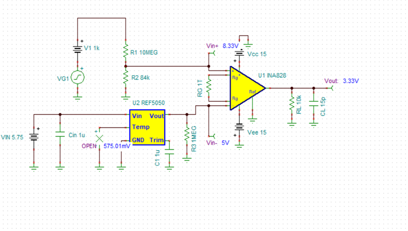
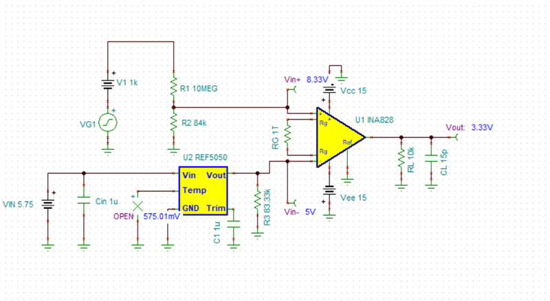
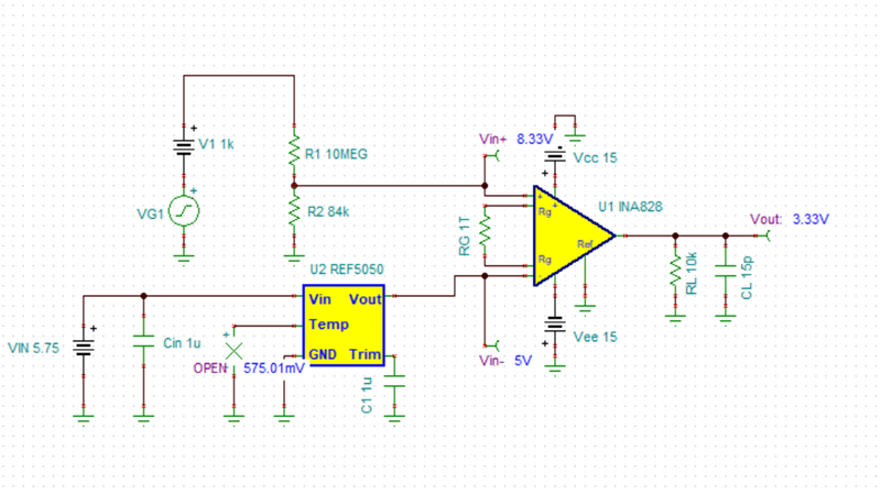
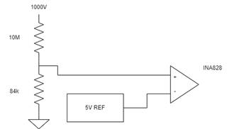
Here is how my input stage looks:

 As far as I can tell there needs to be a path to ground for both inputs. The non-inverting input has a path through the 84k albeit the inverting input doesn't. 

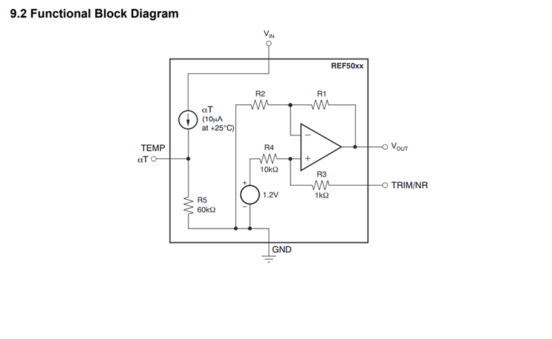
1) Do I need to add a resistor to ground at the output of the 5V ref? I'll be using REF5050

2) Is there a sufficient path through the 84k for the non inverting input?

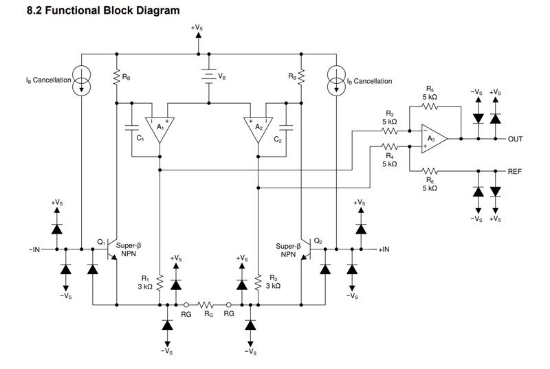
Additionally, I understand that the Darlington pair at the input will draw a current to bias the transistor, this will be drawn from the circuit attached to the input, I just dont quite understand why there isnt an internal path.

3) Is this dependent on what is connected to the input and it's source impedance?

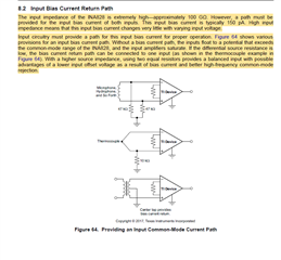
It is also very interesting that their is an input bias current cancelling current source to provide a base bias current.

Lastly I have watched the precision labs videos and read a few app notes but cant seem to figure it out. Any assistance will be appreciated.

  • Hello, 

    I have simulated the basic circuit that you provided and added a 1M resistor on the inverting terminal to ground for a return path. I see the expected 8.33V on the non-inverting terminal provided by the 10M and 84k resistor divider. I don't see a return path problem via the 84k resistor. 

    Free TINA Ti download:

    https://www.ti.com/tool/TINA-TI

    Simulation File: 6403.INA828.TSC

    The bias current is the same regardless of what source is connected to the INA. However it is important to know your source impedance because the input current noise gets multiplied by the source impedance and translates into additional voltage noise. Bipolar input stages have higher input current noise than that of their JFET and CMOS counterparts. The bipolar inputs are great for their low voltage noise characteristics and when paired with a sensor that has low source impedance the bipolar amplifiers are a great choice. There is a breakaway point in the source impedance value, when choosing a CMOS or JFET device is better suited. For this reason it is important to know your source impedance over frequency. I recently wrote an application note on the subject that can be found below. 

    Ultra-Low-Noise JFET Preamplifier Design for High Impedance Sensors:

    https://www.ti.com/lit/ab/sboa589/sboa589.pdf?ts=1722278379832&ref_url=https%253A%252F%252Fwww.ti.com%252Fproduct%252FINA849

    Best Regards, 

    Chris Featherstone

  • Hello, 

    To follow up on my last post. You may change the 1M resistor to ground on the inverting terminal to match the impedance seen on the non-inverting node for balancing the impedance on both legs. 

    Best Regards, 

    Chris Featherstone

  • Thank you for the detailed reply Chris, highly appreciate it.

    There are just two things I would like to check:

    1) How did you determine that the size of R3 should be 1 M-Ohm

    2) What would happen if this resistor is not included (any article can be linked if possible) I did watch the TI precision labs which explains this but I did not have an 'ah' moment and would like a deeper understanding nor can I see anything from simulation.

    Thank you Again, i will have a look at the article you linked now.

  • Hi Pieter, 

    I arbitrarily chose 1M for demonstration purposes. However it would be best to match the impedance to the other input pin. In other words whatever the Thevenin equivalent resistance is that is on the non-inverting terminal which happens to be the 10M//84k which is about 83.33kohm. See the new simulation below:

    The input is a bipolar transistor (shown below) which is a current controlled device as opposed to a voltage controlled device. Therefore a current path to ground must be provided. I don't have an article that goes into detail on this unfortunately. 

    Below is the block diagram for the REF5050 and you can see that there is a current path from Vout back through R1 and R2 to ground. This may be sufficient however it couldn't hurt to add a place holder resistor on the output of the REF5050 to ground to avoid spinning a board. 

    I have checked this in simulation and get the same result as with the resistor. I would recommend having a placeholder on the board however just incase you find you need it. 

    Best Regards, 

    Chris Featherstone

  • Thank you Chris,

    Appreciate all the assistance