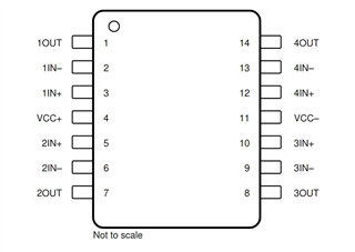
This thread has been locked.

If you have a related question, please click the "Ask a related question" button in the top right corner. The newly created question will be automatically linked to this question.

TL074H: ESD diode

Part Number: TL074H
Other Parts Discussed in Thread: TL074

Tool/software:

Team,

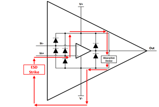
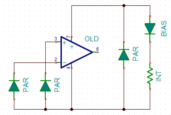
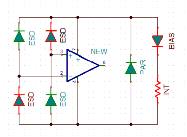
I'd like to know what is the topology of the ESD diode inside the TL074H. Customer plans to do the ICT(Initial circuit test) test at ESD diode in the production line. Is below diagram identical to TL074H? Or what else diagram you can share? very thanks. 

  • Brian,

    All the diodes shown are present in TL074H, there may or may not be a resistor in series with input resistors. 

  • So, there're four ESD diodes as diagram i shown. How about the absorption device? Is it integrated in the TL074H? is it TVS?

  • Brian,

    I can say TL074H acts like a diode for V+ < V- voltage. Do not under any circumstance try to turn on the absorption device in any op amp during ICT. This is a really bad idea. 

  • Thanks Ron.

    Customer would like to know the internal diode topology in the TL074I and TL074H. Does both have the same ESD diode structure? 

    Since customer found 3 parts TL074IDR were failure during manufacturing with ICT test (42C0PCK => NG, 37A5EJM => Pass).

    Are both ESD diode identical design with diff. assembly site as blelow?

    ASO

    CSO

    AssyLTC

    MLA

    RFB

    42C0PCK

    MEX

    SHE

    37A5EJM

    Regarding to the ICT test, DELTA is using ICT probe measured between PIN2 to PIN1, and PIN6 to PIN1. is this probe position ok or not?

    Or using PIN1 to PIN11 and Pin2 to PIN11? Customer would like to know which parameters or factors could have impact on ICT testing?

    Regards

    Brian

  • The absolute maximum ratings show that devices in the NS or PS packages do not have clamping diodes to V+. But as far as I can see, you are using the D package.

    PCN# 20221219006.1 introduced a new die for the TL074 (similar to the TL074H die). The guaranteed datasheet limits have not changed. What exactly are you measuring, and what is the failure threshold?

  • Thanks Clemens.

    Regarding to the ICT test, DELTA is using ICT probing measured between PIN2 to PIN1, and PIN6 to PIN1 to check if soldering/component placements on the PCB correctly during manufacturing.

    However, there're three TL074I units failure found at ICT station that die made from RFB(CSO Richardson, US). and they don't find any failure die made from SHE(SHERMAN, US). We're suspect that the new silicon is more weak or not?

    - Are TL074I chip the same process and identical circuit design from both wafer sites of SHE asnd RFB?

    - In the datasheet, it looks the process and design are changed between datasheet when we take look at Rev.V and Rev.S. The new process is by CMOS, old one is Bipolar, correct? 

    - Could you let me know what exact info. you need for this issue clarifying ? Very thanks. 


    In the application, the TL074IDR below is for the voltage sensing. Could you check if it's ok or not? The circuit has been using for a long time in motor drive application. i think it should be ok.

    Please help on this support as it's an urgent case in manufacure site.

    Regards

    Brian

  • The SHE and RFB dies are very different. The old die used JFET inputs, the new die is a pure CMOS device.

    "ICT probing" does not tell me anything. Is it measuring the resistance? What is the expected and the actual value? (There is a resistor between pins 1 and 2, so what has this to do with the opamp?) Is the opamp powered during this test?

  • Hi Clemens,

    Thanks. As i understanding ICT is to use an electrical probe tests a PCB and checks for faultiness such as shorts, opens, soldering problems etc. and it's tested without powering the OPA. And it could be tested with Diode mode of the multi-meter. However, if I can get the exact test condition of the ICT from DELTA manufacturing site, i'll let you know

    ICT testing; ICT probe measured with diode mode between PIN2(IN-) to PIN1(OUT), and PIN6(IN-) to PIN1(OUT). is this ok?

    It looks the device from RFAB with CMOS that is more sensitive to ICT testing and easy to be damaged comparing to JFET inputs from SHE, right? if so, why?  

    Regards

    Brian

  • I would expect that the ICT limits the current to a safe value. But I do not know what "failure" means in this case; is the device actually damaged?

    I do not understand why there is a test between the input and output pins. Some current will flow through the feedback resistor, and there is no direct internal connection between these pins. If you want to check for the ESD clamping diodes, do the test between any of the I/O pins and any of the power pins (4 or 11).

  • Customer would like to know the internal diode topology in the TL074I and TL074H

    Older TL074I is like this; "PAR" is parasitic diode  

    TL074H is like this; "ESD" is ESD cell 'diode'.  Newer TL074I could be like this too.