This thread has been locked.

If you have a related question, please click the "Ask a related question" button in the top right corner. The newly created question will be automatically linked to this question.

JFE2140: JFE2140 capacities

Part Number: JFE2140
Other Parts Discussed in Thread: TINA-TI, JFE150, STRIKE

Tool/software:

Hi,

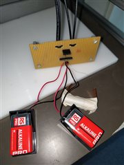
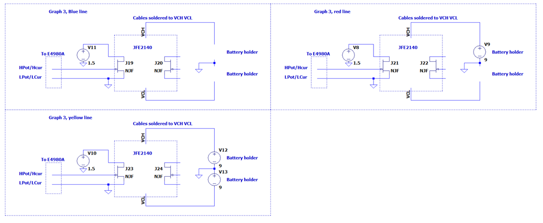
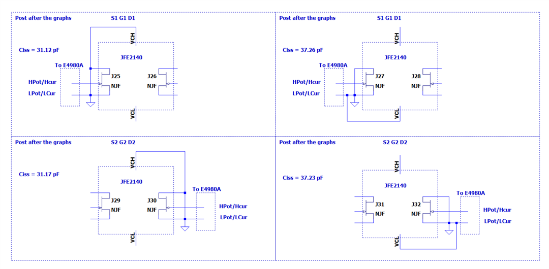
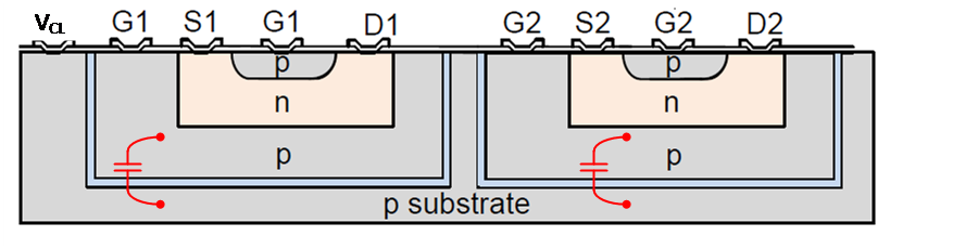
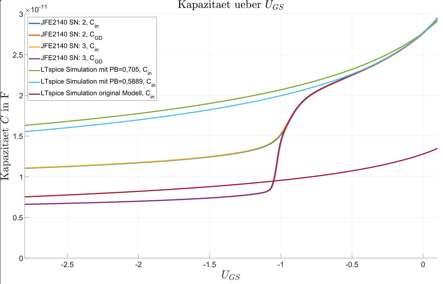
we are currently evaluating the JFE2140 and noticed a relatively big discrepancy between the Spice-Model and the real capacitances (Gate to Source and Gate to Drain) which results in a lot of additional noise in our application.

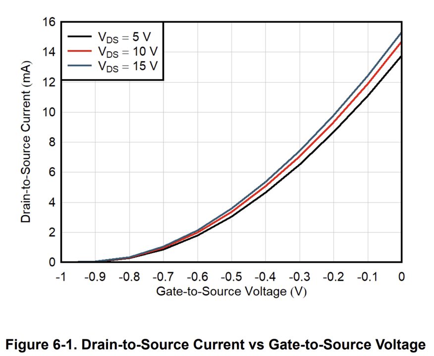
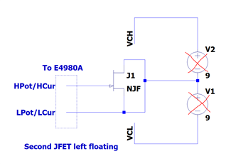
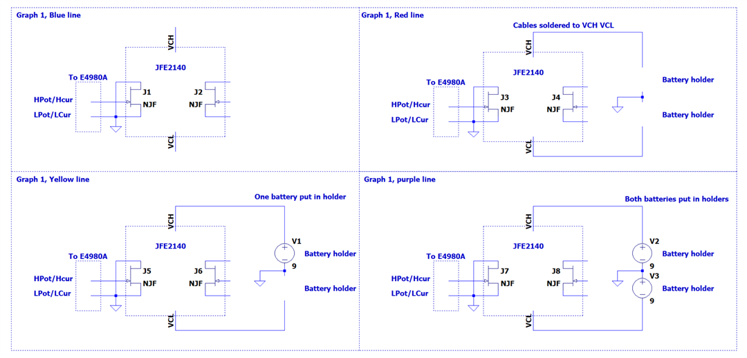
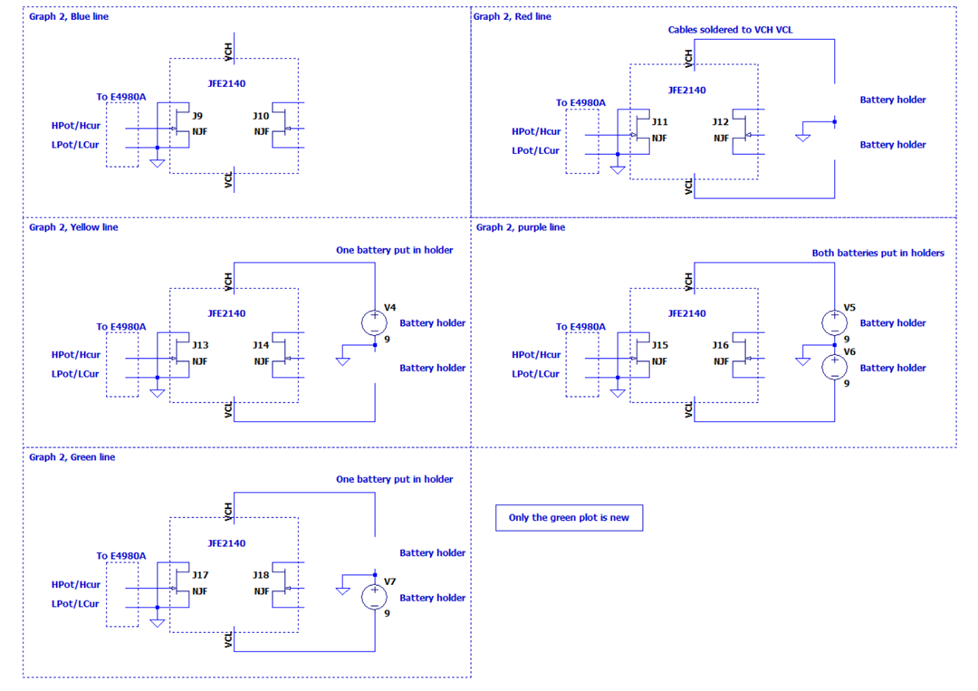
The datasheet lists some capacitances in figure 6-17 but sadly without noting at which gate voltage these measurements  were taken. When measuring the capacities with an E4980A, it seems like figure 6-17 gives the capacities for roughly >0.7 V gate-source voltage.

Is there more specific data available regarding the different capacities over a broader range of gate voltages? The Spice Model (using the PSpice parameters in LTspice) tells a completely different story, one which needs roughly 5 pF additional Gate-Drain and another 10 pF Gate-Source to comply with the results we are seeing in the real world.

Can someone confirm these higher capacities and the misleading behavior of the Spice models?

Best regards,

Gerrit

  • Hi Gerrit, 

    How are you testing the capacitance in your simulation? If you can demonstrate your results and the circuit I can run this by our modeling engineer. 

    We verify our measurements against design and these should all align with the model. I recommend checking your results in Tina Ti against your other simulation. Tina is a free download that can be found here:

    https://www.ti.com/tool/TINA-TI

    The IDS current is 2mA and the VDS voltage is 10V. The VGS is therefore -0.6V

    This is in alignment with my Tina Ti simulation:

    The noise analysis below lines up with our measurements. 

    Best Regards, 

    Chris Featherstone

  • Hi Chris,

    thank you very much for the quick reply. I will try the simulation in TINA-TI and report back to you in a couple hours.

    The problem we are facing is too much current noise on the gate of the JFET at high frequencies ( upwards of 10 kHz). We checked the voltage noise on drain and source and they look fine, exactly as in the simulation.  As the noise is rising with frequency it seems to be some kind of enC noise, which we can reproduce in the simulation by adding the mentioned capacities.

    My colleague with a better understanding of low capacitance measurements and more experience in using the E4980A will be in house tomorrow, so the measurement is preliminary. But I measured 19 pF Gate-Source capacity at 1,4V Drain-Source voltage and a Gate-Source Voltage of -300 mV. Simulation lists values < 10 pF for those operating conditions.

    I will get back to you with more information once I finished checking things in TINA-TI and talked to my supervisor regarding how much I am allowed to share, as company policy regarding this stuff is on the tight side.

    Best regards,
    Gerrit

  • Hi Chris,

    i rebuilt the input stage in TINA-TI and I am getting almost the same results as in LTspice - definetely close enough.

    So my LTSpice simulation seems to be correct. I will play around with the capacity simulations a little bit later.

    But while thinking about my problem, the protection diodes came to my mind. As we found them to be too leaky, we chose external diodes and left them floating - as stated in the datasheet.

    Therefore they are not actively reverse biased and their space charge region would be rather small - in turn giving me a big capacitive coupling between the two gates of the JFET. That could - although we are talking about 10 pF and larger - potentially explain the deviation I am seeing.

    I am going to check this in the lab in a couple of hours and get back to you about it. It would of course be nice to hear your thoughts about my theory. Next question would be where to place VCH and VCL, as the nodes of course will need to be very quiet. 

    Regarding your question about capacity in the Simulation - LTspice can provide the Gate-Drain and Gate-Source capacities for a calculated DC-Operating point. Thats where I got them from. Still looking for the same function in TINA-TI to further verify the LTspice Simulation.

    Best regards,
    Gerrit

  • Hi Gerrit, 

    The protection diodes have approximately 1 pF of additional capacitance. Here is a snippet from the JFE150 datasheet.

    Best Regards, 

    Chris Featherstone

  • Hi Chris,

    i am in doubt about that capacity value the datasheet specifies. Therefore I am currently trying to build a setup that can sweep Vds and Vgs at the same time to measure the capacity over the whole operating area.

    My suspicion about the diode capacities beeing the problem seems to be partially true, but as I can not explain the effects we are seeing when connecting the diodes I will get back to you on that topic once I gathered more data.

    Can you tell me more about the setup you are using for capacity measurements, so that I can replicate that to the best of my abilities?

    Can you recommend a book or a set of papers that explain in depth the effects that can be seen in JFETs (variation of capacities, gate leakage, noise theory etc.)?

    My supervisor sadly denied the sharing of  schematics in this public forum, so in case I can not confirm the higher diode capacities, I would like to switch this discussion to an email-based form, but the measurement side of things will continue here.

    Best regards,

    Gerrit

  • Hi Gerrit, 

    I have reached out to our design engineer for the JFETs. He is in Germany so there will be some delay in responding to these questions. When it comes to the internal diodes and capacitance of the JFET diodes I will need to rely on his expertise to provide guidance. I will ask our validation team for guidance on the test circuit. 

    We have a section on noise theory for op amps in the link below. We don't have a section on noise at the transistor level though. Grey and Meyer or Sedra and Smith texts would go into further detail at the transistor level. The JFETs and CMOS devices use the same small signal models. 

    https://www.ti.com/video/series/precision-labs/ti-precision-labs-op-amps.html

    Best Regards, 

    Chris Featherstone

  • Hi Gerrit, 

    Here is an IEEE paper on making these measurements.

    https://core.ac.uk/download/pdf/39240543.pdf

    Best Regards, 

    Chris Featherstone

  • Hi Chris,

    thank you for the link that explains making theses measurements. Before going all in and building the testcircuits in full glory, I did a couple measurements this morning with the following circuits:

    I started with the simplest one, Drain-Source shorted together, measuring the Gate capacity. The drain connection was later cut and a voltage source with 1.5V was added going to source. All measurements were taken using a Cp-Rp model with 10 mV amplitude at 1 MHz.

    The red crosses are the points where the connection is cut, when the following graphs say "VCx open". The biasing of for VCH and VCL is achieved with 9V batteries, as I got a lot of capacity fluctuations when using a SMU (B2901A). Therefore I can only provide sweeped Gate voltages, all other voltages are fix for the moment.

    Next picture additionally shows the version with open VCH:

    And to see what a change in Drain-Source voltage does, I used a 1.5 V batterie to bias Vds, giving the following results, which are not surprising (i am not sure why they are so rough in places):

    This behavior when biasing VCH and VCL does not fit my (and that of my colleagues) understanding of diode capacity over bias voltage. We would have expected a reduction in capacity as the bias voltage should widen the depletion zone and therefore effectively reduce the diodes capacity - which should lead to a lower overall Ciss.

    These measurements seem quite implausible, but i also measured a LSK489A and the capacity sweep almost perfectly aligns with the one given in it's datasheet.

    If you have further questions about my measurements, do not hesitate to ask. The build is rather ugly, but I will show it in case it leaves open any questions:

  • The capacity of the protection diodes seems to be rather constant. A measurement with VCH and VCL shorted to Source and also Drain shorted to Source yields a input capacity of 37.29 pF at a gate bias voltage of 0 V (no sweeping possible as i would quickly run into forward biased diodes)

    For S1 G1 D1 (the same as in the graphs above)

    Only shorting VCH to Drain and Source yields 31.12 pF (a second JFE had 31.44 pF)

    Only shorting VCL to Drain and Source yields 37.26 pF (a second JFE had 37.25 pF)

    For S2 G2 D2

    Only shorting VCH to Drain and Source yields 31.17 pF (a second JFE had 31.28 pF)

    Only shorting VCL to Drain and Source yields 37.23 pF (a second JFE had 37.29 pF)

    So they are indeed symmetrical in that regard, but the Diodes add quite a bit of capacity and that rather regardless of the bias voltage. This reminds me of a thread i read here where someone complained about the rather high capacities of these diodes. Seems like he was kind of correct and the datasheet claim of ~1 pF is not that real.

    The diodes (especially the VCL diode array) seem to add a rather constant 10 pF to the gate capacity, regardless of a 9 V biasing or 0 V biasing.

    This does not seem to be a pn-junction, rather something more like a traditional parasitic capacitance (can't be the bond wires, 10 pF in that small package would require tiny distances wire to wire, same goes for the pins), so my guess would be something else going on with the internal layout. This is sadly all i can really do from an investigative point of view, as further troubleshooting or verification would require more knowledge about the internal layout (I would really like to do that, but I doubt that you would just send over the layout, but feel free to do so :)  ).

    Best regards,

    Gerrit

  • Hi Gerritt, 

    I am trying to follow along with your test. Are these measurements made when the protection diodes internal to the JFE2140 are floating meaning they are disconnected?

    Best Regards, 

    Chris Featherstone

  • Hi Chris,

    the graphs say if they are floating. VCx open means they are floating, if there is a voltage stated, then they are connected. Cables soldered means that the cables to the battery holders are soldered on (only the first measurement is without them), but no batteries are inserted yet. Through the capacity of the cables, there is already a little bit of a "grounding/not so floating for high frequencys anymore" effect. Thats why i showed it there.
    My second (and last post) then went ahead and removed all external biasing (except for the gate biasing, which is done by the E4980A) and connected VCL or VCH to The source/drain contact, which were shorted together.

    I hope this clarifies things a little bit. I am drawing a couple of schematics and will attach them in a few minutes.

    First image in the graph post:

    Second image (only the green line is new)

    Third image

  • And for the post without graphs:

  • Hi Gerrit,

    Only shorting VCH to Drain and Source yields 31.12 pF (a second JFE had 31.44 pF)

    Only shorting VCL to Drain and Source yields 37.26 pF (a second JFE had 37.25 pF)

    For S2 G2 D2

    Only shorting VCH to Drain and Source yields 31.17 pF (a second JFE had 31.28 pF)

    Only shorting VCL to Drain and Source yields 37.23 pF (a second JFE had 37.29 pF)

    Are you saying that the unbiased diodes are adding the capacitances that were measured here? In other words the unbiased diodes alone are adding 31-37pF?

    Best Regards, 
    Chris Featherstone

  • Hi Chris,

    not exactly. The values given there are absolute gate capacities, one would have to subtract roughly 27.8 pF from those values (that is the measured gate capacity with shorted Drain-Source and floating VCL and floating VCH

    Best regards,

    Gerrit

  • Hi Gerrit, 

    The blue layer below is an SiO2 layer. When biasing VCL with a DC voltage this looks like AC ground and a capacitor is formed between the gate and the p-substrate. For this reason you will seen an increase in capacitance when the diodes are biased. The capacitance values in the datasheet are with the diodes floating and not connected. We do not model the diode capacitance in the spice model. 

    There is a diminishing return on noise when running the JFETs with a lot of current. In fact at at certain point the thermal noise will increase as seen below. 

    Keeping the VDS lower as shown below will minimize the rise in gate current. 

    Best Regards, 

    Chris Featherstone

  • Hi Chris,

    thank you very much for the cross-section. Now the things we are seeing make a lot more sense (different configurations of the input stage showed different input capacities) since input capacity on one gate depends on the potential and movement of the other gate.
    That is very unfortunate, as this effectively makes the capacity in circuits where differential signals are applied to the two gates of one package much larger than in the datasheet and also much larger than in the simulation. So we won't be able to use the JFE2140 as intended.

    It might be worth changing the Spice Model for a dual version that incorporates this behaviour and/or mention the fact in the datasheet, as that would have saved a lot of time and at least one revion for us.

    Thank you very much for your quick and in depth help with our problem.

    Best regards,
    Gerrit

  • Hi Chris,

    this resolved my issue mostly, so the noise is now in a more acceptable area.

    Something that is now a problem/task at hand is the binning of those JFE2140. They all have - as it seems - unique numbers printed on the back side of the package, for example 01N32 with the last two digits counting up. Do you know if the respective dies were next to each other on the wafer, if I have the 01N32 and 01N33? That could be a great start for binning measurments as we would assume that tolerances are tigther when the dies come from a smaller area on the wafer.

    Thanks again for your superior support.

    Best regards,
    Gerrit Schlüter

  • Hi Gerrit, 

    Usually a tube of devices would have die that are next to each other. However there is no guarantee they would be from the same column so as you move up the wafer at some point parts come from the next column over and down. This makes it challenging to rely on for binning. I reached out to our project management on the numbers you referenced. They are mold cavity location numbers. 

    I did provide your feedback on the diodes to our team. So we do have that on our minds for the future. Sorry for the inconvenience on this! We were kinda tossing the idea around of putting a TVS in series with VCL and ground or a negative voltage so that it is only connected during an ESD strike. We don't have any data on this though. Just a thought we had as a work around for now. 

    Best Regards, 
    Chris Featherstone

  • Hi Chris,

    thanks for the information about the mold cavity numbers. It would be very interesting to hear what your project management says about the numbers, as they don't align with the Spice models numbers (which seem wrong, as they also dont' match the datasheet numbers). I fitted the model to my measurement results, but a confirmation would be nice.

    The idea with the TVS diode would not solve the problem sometimes. In for example a differential input stage, you would see the same input capacity regardless of using a TVS diode or a fixed low impedance potential, as with a symmetrical input signal, those gates would move in opposite directions, leaving the VCL potential the same. As for something like a non inverting amplifier, your suggestion would indeed be helpful.

    Just my personal opinion: Those clamping diodes are a nice feature, but for now i think they do more harm than good. The leakage current is way higher than that of something like a BAV199. Those JFE2140s are really nice JFETs compared to the other available products, with the only downside beeing the capacitive coupling between the gates of the two JFETs. Solving that and just leaving out the Clamping diodes would be a huge upgrade (it can be done, Interfet seems to be able to do that). Just mentioning the additional capacities in the datasheet and model would be a great thing for now in order to help other designers not run into the same problems.

    Best regards,
    Gerrit Schlüter

  • Hey Gerrit, 

    Thanks for the feedback! I have provided the information back to our spice modeling engineer as well. We generally provide behavior models as opposed to a replica of the device in simulation. For example on the op amps you may not get perfect Vos vs Vcm or Vos vs Vout sweep data implemented in the model that describes the "knees" as we call them. This is the curvature behavior when going from the linear operating points to non-linear. In the instance of the JFET I can definitely see where the extra capacitance can be helpful however and potentially not a tough ask to add to the model. At a minimum I agree that we should add this information to the datasheet. Although you may have given us some ideas to write another app note that could potentially go deeper into this topic. Your feedback is valuable and there are several people in the group I have made aware of this issue. 

    Best Regards, 

    Chris Featherstone

  • Hi Gerrit, 

    I had just a few things to add regarding the JFE2140. One of the biggest benefits with the JFE2140 is the matching between the JFETs. Both JFETs are on the same die and share the common substrate. It is the common substrate creating the capacitance and not the diodes. A lot of N-ch JFETs on the market are just to separate JFET dies in 1 package. This has the advantage of less capacitance because relatively speaking the the two parts are much further apart. However the matching between the two JFETs is not as good as the JFE2140. 

    Best Regards, 
    Chris Featherstone

  • Hi Chris,

    seems lik I did not hit reply after typing part of this message a couple weeks ago.

    That is true and I get your point and the JFE2140 is a rather excellent JFET after all.


    Did you hear back from your project management regarding the capacities I measured?

    I did a few more measurements regarding the JFE2140 in order to fit the Spice Model to the real world measurements. I had to change CGD and CGS and also PB in order for the model to fit the measurement data in the region for draincurrents of 2 mA and above.

    At the end the real world performance is what matters, but as the simulations will be part of a scientific article/thesis, it would be nice to get some kind of confirmation about it.

    Following this document from InterFET, I fitted the CGD and CGS to my measurement results. That alone fixed the models capacity for 0 V Vgs voltage (as expected). Calculating the necessary PB for the measured results at -0.5V resultet in PB=0.5889, so my overall model for the JFET (DJFEx140 Diode stays the same) is:

    .model NJFE2140 NJF (BETA=14.24m BETATCE=-0.22 VTO=-975m VTOTC=0.45m LAMBDA=11.9m RD=10 RS=8 N=1 M=0.33 PB=0.5889 IS=5.34f CGD=11.1711p  CGS=16.4289p AF=1 KF=0.2e-18 FC=0.5)

    Simulating the model capacity with drain and source shorted together gives a pretty good approximation and fits the measured results rather well.

    The graph (sorry for the german labels. Our 0,705 is your 0.705) shows capacity on the y-Axis and the Gate-Source-Voltage on the x-Axis. It shows the measurements (first four points in the legend), in green the simulation with CGD=11.1711p  CGS=16.4289p but PB=0.705 and in light blue with PB=0.5889. Last point in the legend is the original JFEx140 model from TIs website.

    Measurements were taken with two different JFE2140 to make sure it is repeatable.

    1. Measure sweeped Cin (Gate capacity to Drain AND Source)

    2. Measure sweeped Cgs (Drain is open. Measures Cgs only until channel gets conductive)

    3. calculate ratio of Cgs to Cgd from data in the area -2.8V to -1.5V

    4. Use Cin at Vgs and the ratio from 3. to approximate CGS and CGD for the spice model

    5. Tweak PB to fit the Model to measured data

    Is there any obvious problem with these measurments from your point of view?

    Best regards,
    Gerrit Schlüter