This thread has been locked.
If you have a related question, please click the "Ask a related question" button in the top right corner. The newly created question will be automatically linked to this question.
Tool/software:
hello.
I configured a paralled operation circuit with reference to Figure.15 in the Application of OPA541.
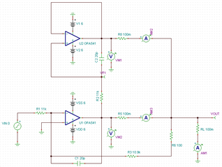
+VS: +6V, -VS: -6V
R1: 10K, R2: 10K
I set the input power to -1V and set the 5A in the loader instrument, it will be 1V/5A setting in the output.
Current Sharing of Master Opa541 and Slave Opa541 work well
but
I set the input power to +1V and set the 5A in the Loader instrument (polarity change), the output is -1V/-5A setting.
Current Sharing of Master Opa541 and Slave Opa541 do not work well.
The Master OPA Output Voltage starts with -1.45V and Slave -1.0V, and after about 30 seconds, it changes the same to 1.0V and 1.0V.
I want to check if this is normal.
And additionally 10A output is not available on SOA in that paralled operation circuit(+6Vs, -6Vs, 1Vout)? Is it possible up to 7A?
Hi Seokbong,
This delay may be caused by the a few reasons. Is the load purely resistive, or is it also capacitive/inductive?
C1 and C2 sometimes require optimization to ensure proper circuit operation. Would you be able to remove the components for a quick test on your board.C2 can especially cause problems sometimes for parallel circuits like this.
Does the amplifier set to -1V faster if you reduce the current load?
Thanks,
Jacob
This delay may be caused by the a few reasons. Is the load purely resistive, or is it also capacitive/inductive?
-> My loader instrument set Resistive
C1 and C2 sometimes require optimization to ensure proper circuit operation. Would you be able to remove the components for a quick test on your board.C2 can especially cause problems sometimes for parallel circuits like this.
-> tested C1, C2 but the results are same
Does the amplifier set to -1V faster if you reduce the current load?
-> Yes. The speed was fast on the low current.
Hi Seokbong,
Thanks for the details here.
Do you have bypass capacitors on the supply rails of the amplifier?
Layout like this will provide a low impedance path for transient return currents to pass back to the supply pins of the device.
A good place to start would be taking scope shots with low current and full load at a few points on the circuit. These scope-captures will help me understand what parts of the circuit are operating as expected.
If possible, could you please place probes at the following nodes:
Vin
IN- U1
Vout U1
Vout U2
Seeing the transient response at these nodes will help us possibly understand what is going on.
Thanks,
Jacob
Thanks. Jacob.
spcope captures here.
load set 6A, then U1 vout is -1.4V and U2 vout is -1.2V.
Hi Seokbong,
Thanks for the scope shots, I appreciate you taking this data for me.
I cannot tell if U1 Vout and U2 Vout are really 200mV different, but I can clearly see that there is a time delay associated with the realization of the final value.
As I see it, it looks like the output first goes to -.9V for U1 out and U2 out, then after about 4 seconds goes to -1.4V. Do you see things the same or different?
Thanks,
Jacob