This thread has been locked.

If you have a related question, please click the "Ask a related question" button in the top right corner. The newly created question will be automatically linked to this question.

OPA541: OPA541: Paralleled Operation for the OPA541 V2

Part Number: OPA541
Other Parts Discussed in Thread: OPA549, OPA452, OPA548, OPA547

Hi Thomas Kuehl,

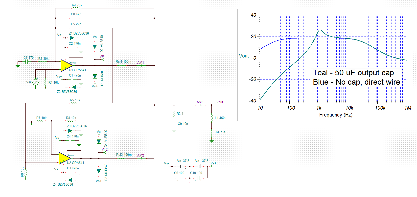
I take my previous subject (which was closed) "OPA541: Paralleled Operation for the OPA541"; additional data that can change a lot of things: I told you that the load was "The load: It's a coil of 1.9H with a resistance of 11Ω which we can add cable resistance, at the maximum 40Ω.". There is a modification, here is the real charge "The load: It's a coil of 0,46H (about) with a resistance of 1.4Ω (about) which we can add the cable resistance, at the maximum ." It is totally different.

I did the test with my previous schematic, in different steps :

- First, I simulate my load with a resistance on the output of 180Ω if I remember. My signals were OK.
- After, I plugged the real load : a coil of 0,46H with a resistance of 1,4Ω. It wasn't worked (my amplifiers were heating up and my signal was distorted). I can join you pictures if you want.

Thank you for your answer.

Regards.

  • Hi Florian,

    A 180 Ohm load is a very light, very different load, than a 0.46 H inductor having 1.4 Ohms resistance. Please send an updated schematic showing the OPA541 circuit, the output load connection including any cable and its characteristics, power supply information, and input signal information. Images of the input and output signals are needed as well.

    Regards, Thomas

    Precision Amplifiers Applications Engineering

  • Hi Thomas,

    Please find in attached :

    • The updated schematic.

      OPA541_noninv_parallel_07(modif).TSC

    • The load is a coil of 0,46H with a resistance of 1,4Ω which can be, in the worst case, 4Ω (adding the cable resistance). The cable is a shielded cable, twisted pair of 2,5mm².
    • Power supply : my circuit is powered by +/-36,8V
    • You can find also 2 images : the first one is the input and output with a 180 Ohm load, the second one is the input and output with the real load (0.46 H inductor having 1.4 Ohms resistance)

    Regards

  • Hi Florian,

    The OPA541 TINA simulation circuit you provided indicates that the input signal is a 4.4 Vpk, 1.2 kHz sine wave. I believe the waveform presented on DSO channel 1 confirms that is the approximate input condition.

    When I analyze the 0.46 H load, it has an inductive reactance of almost 3.5 k-Ohms (j3500) at 1.2 kHz. This is accompanied by a small series resistance of 1.4 Ohms. Therefore, the output load is almost entirely reactive. The circuit is set up for a voltage gain of 8.2 V/V so for a 4.4 Vpk input the expected peak output voltage would be about 36.1 Vpk. That would be a problem.

    If I lower the peak input voltage such that the output is within its linear range the current is surprisingly low. For example, if the output is kept to 30 Vpk, the current is only about 30 Vpk/ 3500 Ohms, or 8.5 mA peak, for the reactive load. That is actually a much lighter load than the 180 Ohm resistor poses, which would draw about 170mA.

    When a TINA simulation is attempted with the 0.46 H reactive load it indicates that the output is hitting the rails which causes the simulation to stop. It appears that the gain is too high and also there may be some gain peaking occuring because of the circuit Q. You mention the twisted pair cable. That is adding some capacitance across the inductor and adds another reactance to the load. If I reduce the input voltage down to 4 Vpk, then the output doesn't hit the rail and simulation finished. Try reducing the input voltage and see if the distortion decreases.

    You may find it necessary to reduce the drive slightly, or decrease the gain slightly, and add some resistance across the inductor to lower the Q so that the output voltage remains within the linear range of the OPA541.

    Regards, Thomas

    Precision Amplifiers Applications Engineering

  • Hi Thomas,

    As you said, I decreased the gain slightly (now R4 = 12K and R3 = 1,8K). Now, when I simulate my circuit, no problems.

    But in reality, it's different. When I connect my load (the coil), my signals (input and output) are totally distorted, worst than before. I really don't understand where does the problem comes from.
    It's strange, it's as if there was a return of the output on the input.

    Regards,

    Florian

  • Thomas,

    After checking, this is the 2 signals (input and output). Output signal looks a liitle bit better than last time, but he is still distorted. And my input signal hasn't the same amplitude with and without load. I don't understand.

    Regards, Florian

  • After my load, my signal comes on my board for digital processing; We use a 0,05 Ohm (1W) resistor to read the current. Can my resistance be poorly sized?(Power too less?)

  • Like this :

  • Hi Florian,

    It appears that the upper NPN output transistor is turning off momentarily. You are driving the ouput swing to the maximum and beyond and there may not be enough voltage remaining to keep the current source and output Darlington turned on during that portion of the waveform. Remember you are driving a complex impedance and the peak current and peak voltage are out of phase. Try reducing the drive and see if the waveform returns to a sine wave, or if you have the option of increasing the supplies try doing that.

    Regards, Thomas

    Precision Amplifiers Applications Engineering

  • Hi Florian,

    Is the 50 m-Ohm resistor connected across the 0.46 H/0.4 Ohm load? I don't see how that could be the case. The current required by the resistor would be many Amperes, and it would need a power rating much higher than 1 W. Please clarify.

    Regards, Thomas
    Precision Amplifiers Applications Engineering
  • Hi Thomas,

    I can't reduce the drive, because the signal comes from a microcontroller, and the amplitude is fixed. I can try to reduce the gain again?

    If I increase the supplies, does it will work?Because the value of my TVS is 36,8V, same as my supplies. So if I increase my supplies, I have to change my TVS also?

    Regards, Florian

  • Thomas,

    This is how the resistor is connected. I need many amperes, that's why I use two amplifiers in paralell.

    Regards, Florian

  • Hi Florian,

    You would have to increase the TVS voltage; otherwise, they might turn on which wouldn't be good. But you could just remove them for the test with the higher supply voltage level.

    Regards, Thomas
    Precision Amplifiers Applications Engineering
  • Hi Thomas,

    As you said, I removed the TVS and I increased supply voltage. I tried with +/-37,3V, +/-38,3V and +/-38,8V.
    I still have the same problem :

    I don't want to increase the supplies too close to the maximum power supply voltages.

    Regards, Florian

  • I did two others tests. For the two, supplies is always the same, +/-38,8V.

    For the first one, I decrease the gain to 6,55 (I used 10k and 1,8k). The curves looks better, but not stil ok :


    For the second one, I reduced the gain to 5,87 (I used 5.36k and 1,1k). This is the curves :


    The curves looks ok but :
    - The second heats up a lot and very quickly, so it's not normal. Maybe the power supply voltage (38,8V) is too high?
    - When I measure the current with my system, I've about 4,7A. The aim was to use two amplifiers in parallel to have more current than one. With this voltage and current, it's not necessary to use 2. How can I increase the power (voltage and current) in the coil?

    Regards, Florian

  • Hi Florian,

    The OPA541 output voltage does appear to be approaching a peak of 45 V, based on the DSO vertical scale of 20 V/div. That is difficult to understand how that could be the case because the dc supplies were set from +/-37.3 V (74.6 V) to +/-38.8 V (77.6 V). If the output is actually attempting to move higher than the supply rail due to the complex impedance load conditions there may be a brief moment in the output voltage/current relationship where the upper output Darlington turns off. That is what the downward spike is suggesting. Once that momentary condition changes the output resumes operating normally.

    It would seem if the OPA541 output were kept within its specified output swing range, IO = 5 A, continuous ±(|VS| – 5.5) ±(|VS| – 4.5) V, that this downward spike wouldn't occur.

    Regards, Thomas

    Precision Amplifiers Applications Engineering

  • Hi Florian,

    The power dissiaption wil be higher in the second instance because of the lower peak output voltage, relative to the supply voltage. That will result in higher power dissipation and heating. You could try reducing the supply voltage to the point where you still receive a satisfactory peak output level. The power dissipation would be reduced in that case. Attaining the necessary level of heat removal in a power circuit can be challenging. By using two OPA541 instead of one might make the heat removal task a bit more manageble.

    The OPA541 is rated for a continuous current of 5 Amps providing the SOA requirments are met. The OPA549 is rated for a continuous current of 8 Amps. It also features functions such as enable/shutdown that could be used to idle back the power dissipation, and thermal shutdown which protects the output should the dissipation become too high.

    Regards, Thomas

    Precision Amplifiers Applications Engineering

  • Hi Thomas,

    This is due to the resonance of the circuit, that's why output voltage has a peak of 45V.

    But there's someting I don't understand. With our old circuit (we used one OPA549 and the load was a coil of 1,8H and his resistance R=11 Ohm), the output moved higher than the supply rail, and there was no problem with the Darlighton.

    What's the difference between this 2 circuits?
  • Hi Florian,

    There are significant differences in the OPA541 and OPA549 designs and the current limit circuits are quite different. Possibly there is something about the design differences that allows the OPA549 to tolerate the output over-voltage condition without reacting in the same manner as the OPA541. You may find that the OPA541 is okay with the 1.8 H, 1.9 Ohm load.

    If the output voltage is moving beyond the supply rails that indicates that there is a back EMF being generated by the load. That can be a dangerous condition for the output transistors that can result in damage to the amplifier. That is why the fast power diodes are added from the output to the supply rail. They clamp the voltage across the transistor and should keep it from being biased in a manner that protects the output from being damage.

    Please note that this coming week is the Thanksgiving holiday time in the US. I will be away during this time.

    Regards, Thomas
    Precision Amplifiers Applications Engineering
  • Hi Thomas,

    Today I will do the test with the 1,8 H load. My signal is an excitation signal for the coil, that's why we must have a lot of power on the output (several Amperes).

    Regards,

  • For information, this is the reference of the capacitors for the output :
    uk.rs-online.com/.../
    Is the value of Ir too low for my apllication?
  • Thomas,

    I did the test with this settings :
    R4 = 5,12k & R3 = 1,09k so the gain is 1 +(R4/R3) = 5,7
    Without load : Vin = 8,6, Vout = 48V
    When I plug my load (1,9H and 11Ohm), Vin = 5,40V & Vout = 26V about.

    I really don't understand what's happen.
  • Hi Florian,

    I see you have posted the results further down the thread.

    Regards, Thomas
    Precision Amplifiers Applications Engineering
  • Hi Florian,

    I don't think the capacitors are the issue. I am not sure what you mean by Ir?

    Regards, Thomas
    Precision Amplifiers Applications Engineering
  • Hi Florian,

    It seems odd that the input voltage drops when the output load is connected to the OPA541 output. This hints of a current loop issue with the PC board. Can post your curent circuit design so that we can see how everything is configured at this time? Are you using a DSO, or a meter, to measure the voltages? Can you show the input signal and output signal images with and without the load?

    Regards, Thomas
    Precision Amplifiers Applications Engineering
  • Hi Thomas,

    IR : Rated RMS ripple current at 100 Hz, 85 ºC

    Regards, Florian

  • Hi Thomas,

    Please find the design :


    Vin and Vout without load :

    With the load :

    The measured current is 623mA (we use a little resistor on the electronic board to measure the current).

    Regards, Florian

  • Hi Florian,

    Comparing the OPA541 unloaded and loaded output/input waveforms the gains appear to be equal. The fact that the input voltage is dropping to a lower level when the load is attached is unexpected and a reason for concern. I have studied the internal design of the OPA541 to see if there is a plausable explanation for that kind of response. I cannot find anything about the design that would explain it. The input level should not change with the output load conditions.

    Previously it was mentioned that a microcontroller generates the sine-burst waveform. Could something be happening to its output amplitude level when the OPA541 output load is active?

    Regards, Thomas
    Precision Amplifiers Applications Engineering
  • Hi Thomas,

    Yes, I saw that the gain was the same between unloaded and loaded output.

    I don't think that, the microcontroller only generates a waveform, and nothing happens if the output load is active.

    Many points I don't understand :
    - When I changed the load (see the beginning of the discussion), the excitation signal is not the same (about 10V instead of 8,8V) with a loaded output. How can it affect the input signal?
    - How can I calculate the real value of the output current?

    Maybe this amplifier is not suitable for my application?

    Regards, Florian

  • Hello Florian,

    Regarding your questions:

    - When I changed the load (see the beginning of the discussion), the excitation signal is not the same (about 10V instead of 8,8V) with a loaded output. How can it affect the input signal?

    One would not expect the input signal level to change, with a change in the op amp output load conditions. That is not something that I have ever observed with a properly functioning operational amplifier. The input stage of the OPA541 is a JFET differential amplifier and its impedance is very high. It offers a very light load to the source when the non-inverting input is driven as is the case with your circuit. Could you try driving the OPA541 input with an independent low-impedance signal generator and see if the input and output signal levels are different without, and with, the output load attached? If the input and output levels remain about the same, then that might tell us something about the on-board signal source.


    - How can I calculate the real value of the output current?

    That is an involved question, because once you move away from a purely resistive load to a complex load that includes reactance you have to consider the real power (Watts), the reactive power (Volt-Amperes reactive) and Apparent Power (Volt-Amperes). It is a pretty straightforward subject that incorporates the power triangle relationship between these three different types of power. Rather than repeating what is covered nicely on line, see the following tutorial provided by Arrow.com, and copyrighted by Aspencore Inc. Here's the link:

    - Maybe this amplifier is not suitable for my application?

    Well, I am not sure if this is really an issue with the OPA541 power op amp or something else inthe system. I think the complexities introduced by highly reactive load creates much more different and complex conditions than those encountered when driving a purely resistive load. The fact that the output is rising to levels that are very near, or exceed, the power supply rails indicates that there are things are happening in the circuit that fall outside of the normal operating range.

    If you are not obtaining satisfactory results with the OPA541 and OPA549 you may want to consider an even higher power op amp. The OPA541 and OPA549 are TI's highest power op amps and I don't have anything else I can suggest from our line-up. When we run into that situation, then we often suggest having a look at the high power op amps offered by Apex Microtechnology. They offer a wide variety of power op amps that exceed the output voltage and current capabilites of ours. TI has no affiliation with Apex Microtechnology, but mention them as a courtesy.

    Regards, Thomas

    Precision Amplifiers Applications Engineering

  • Hi Thomas,

    I replace my microcontroller signal by a signal generator : now, the input signal is always the same. But I send a continous sinusoid signal ; can it explain why my second OPA541 was very hot with a 5V peak input signal?

    To resume :

    - With the old design (one OPA549) :
    1.9H with a resistance of 11Ω : 900mA input signal ok, output signal deformed. 42V peak (power supply +/-24V).
    0,46H (about) with a resistance of 1.4Ω : 4590mA, input and output signal deformed. (I 'll measure tomorrow to see if the voltage exceeds the power supply rails)

    - With the new design (2 OPA541) :
    1.9H with a resistance of 11Ω : 650mA input signal and output signal deformed.
    0,46H (about) with a resistance of 1.4Ω : 6000mA, input and output signal deformed.


    f I never excced power supply rails with the old design, it can explain why I have problems with the new design, if I exceed the rails.
    In this case, I think I'll change the amplifier with a bigger.

    I tried to calculate the output current with your tutorial. I find a current lower than 1A, so there's something I don't understand.

    Regards, Florian


  • Hi Florian,

    When you change the input signal from sine-bursts to a continuous sine the duty cycle of the output stage increases and the power it dissipates increases.

    Let me see if I can make some progress in determining the load current using simulation.

    Regards, Thomas
    Precision Amplifiers Applications Engineering
  • Hi Thomas,

    I look forward to hearing from you. 

    Regards, Florian.

  • Hello Florian,

    I've spent a lot of time analyzing the OPA541, dual amplifier circuit we have been deiscussing. However, before I did that I analyed the 0.46 H + 1.4 Ohm series load that you need to drive. The results are may be surprising to you.

    When the impedance of the series 100 uF output capacitor, 0.46 H inductor and 1.4 Ohm resistance are considered the calaculated impedance at 1.2 kHz is 1.4+ j3465.6 Ohms, or 3466∠89.97° Ohms.

    That is a high, reactive imepdance and the associated ac current will be low even at moderately high output voltage levels. For example, if the required output is 36 Vpk, the peak current is:

    ipk = Vpk / ZT = (36 Vpk ∠ 0°) / (3466∠ 89.97°) = 10.39 mA∠ -89.97°

    That is much lower current than expected, and shouldn't require a high power op amp but instead one that can provide the required high output voltage swing and moderate output current.

    When I simulated and analyzed the two OPA541 circuit, I found that there was a high circulating current flowing between the two outputs; upwards to 300 mA peak. That may explain why the amplifiers were getting hot when you drove the circuit with the sine wave generator. The circulating current comes about from the master/slave tied output configuation and the voltage offset of the slave amplifier.

    I propose that a different approach using a high voltage, much lower output current op amp be tried. Since all that needs to be provided is an output current of about 10 mA, a HV op amp such as the OPA452 should work, without the need for the master/slave circuit. The OPA452 is usable with supplies up to +/-40 V and is capable of a 50 mA output. If the output current is kept to the 10 to 15 mA peak level, the output swing to the supply rails is about 1.5 V from them. That is much closer than what can be achieved with the high power op amps.

    I've began simulating the circuit below, but am finding something that may or may not be real. The series output load has a resonant frequency of 23.5 Hz and there appears to be a low-level amplitude component in the peak-to-peak output current. That is why the waveform isn't symetrical about zero. That ripple is right around 23 Hz. If this is real, that is an issue that will have to be dealt with.

    I don't know if you want to pursue another path, but I wanted to present you my latest findings.

    Regards, Thomas

    Precision Amplifiers Applications Engineering


  • Hi Thomas,

    An information which will change everything : the coil is not 0,46H but 0,46mH !!!!!

    Regards, Florian

  • Hello Florian,

    That changes everything in terms of the analysis, and drives the design back to the two OPA541 power op amps. I ran a quick simulation of the circuit with the load inductor chnaged from 0.46 H to 0.46 mH. The result is shown below.

    The peak current is now in excess of 6 Amperes and the peak to peak voltage at the load is very high, ~+/-50 Vpk. It appears there is a near resonance between the inductor and the output coupling capacitor. This would need to be examined more.

    Note that I will soon be taking a break for the holidays. I will not be answering anymore E2E posts after tomorrow, and not until the second week of January 2018. Have good holidays!

    Regards, Thomas

    Precision Amplifiers Applications

    OPA541_noninv_parallel_07.TSC

  • Hi Thomas,

    So what about the problem with excessive heating for the second OPA541?

    On the output, I have 2 capacitors of 100µF in serial. Their values has to be changed?

    Can I increase the current on the output?

    Regards, Florian

  • Hi Florian,

    If the current through the second OPA541 is about equal to that of the first, and it has the same thermal envirornment as the first, it should not be getting any hotter than the first. They should share the output power load and heat nearly equally.

    The two series 100 uF output capacitors (50 uF total) are in conjunction with the 430 uH inductor create a resonance at 1.1 kHz in the output circuit. That is very close to the 1.2 kHz input frequency. The result of the resonance is output peaking which is casuing the output voltage to be higher than the predicted closed loop gain of 8.5 V/V (18.6 dB). According to the simulation the overall gain is 20.6 V/V (26.3 dB), and reduces a little at 1.2 kHz to 19.5 V/V (25.8 dB). The apparent gain is much higher at 1.2 kHz than the 8.5 V/V and that is why the output can exceed the supply rails. Operational amplifiers are not normally operated under such conditions.

    If the 50 uF series output capacitor is removed only a small dc level will be present at the output load. This is due to the op amps offset. Removing the capacitor eliminates the resonant circuit setup and the gain becomes exactly 8.5 V/V in the pass band. You can see this result comparing the output voltage vs frequency response with, and without the capacitor. See the plot shown below. I recommend not using the capacitor. Try doing so and see how the circuit behaves.

    The OPA541 is rated for continuous current of 5 Amperes, and a peak current of 10 Amperes. The limiting factor is the power dissipation which must keep the transistor junction temperature below 150 C. Use the Figure 11 Safe Operating Area graph as a guideline.

    I will be on holiday the next 3 weeks. I hope you make progress with your circuit application.

    Regards, Thomas

    Precision Amplifiers Applications Engineering

  • Hello Thomas,

    Thank you for these information.

    I'll do the test when I get back to the office and I'll keep you informed.

    have a nice holidays.

    Regards, Florian

  • Hi Thomas,

    How are you?

    To keep you informed. The circuit works now, I'm just looking for a good heatsink, because actually I use this one and I find that it heats a lot.

    https://uk.rs-online.com/web/p/heatsinks/1686346/?sra=pstk

      (leght : about 150mm for the 2 amplifiers)

    Is it enough? Or do you know a better one?

    Regards,

    Florian

  • Hi Florian,

    We use the AAVID 530002B02500G heat sink on our OPA547/OPA548 EVM. It has about the lowest heatsink-to-air thermal resistance for the TO-220 package that we could find. The datasheet lists a natural thermal resistance of 2.60°C/W, but that can be reduced to 2.0°C/W with a 300 LFM forced air flow. You can find the catalog information on-line about this heatsink, at companies such as DigiKey:

    Also, you can see how we install it on our OPA547/OPA548 EVM:

    Regards, Thomas

    Precision Amplifiers Applications Engineering