This thread has been locked.

If you have a related question, please click the "Ask a related question" button in the top right corner. The newly created question will be automatically linked to this question.

TL072: TL072CDR

Part Number: TL072
Other Parts Discussed in Thread: OPA192

Tool/software:

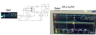
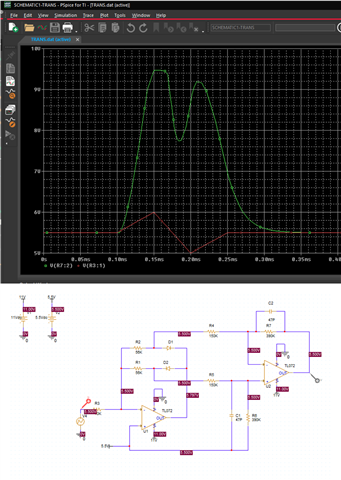
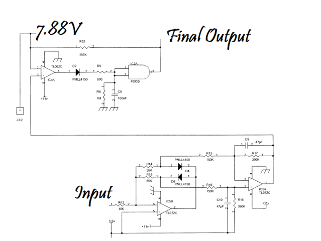
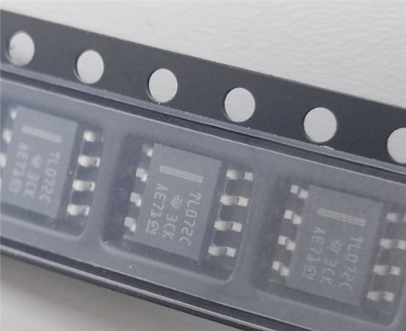
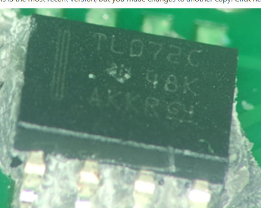
We have procured the TL072CDR part from Malaysia under PCN no: 20220615003.1. However, we encountered a functional performance issue, with 100% of the parts failing during functional testing.

Could you please provide the datasheet details for the parts before and after the implementation of this PCN?

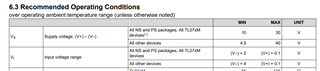
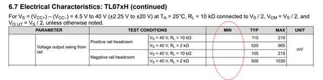
We need to understand if there are any electrical specification differences due to fabrication process changes. Could you please investigate this for us?

To address this issue, we used older parts from Mexico, which were previously procured and placed on boards, and all of them passed functional testing.

This issue has caused a production stoppage. We need your immediate attention.

Thanking you,

Rajani.M

HTS

  • Hi Rajani,

    Overall there are some differences but most performance is better.  It is likely that what you are seeing is a result of the device startup or being measured outside of the recommended operating condition.  The PCN lists some changes and more PCN information can be requested by emailing this PCN support list: "PCN_ww_admin_team@list.ti.com".

    1. VOL, VOH improved (rail to rail output) at open load and most other loads (less than 10mA).
    2. Output current limit is active instead of passive. Output drops suddenly during current limit. Previous was smooth voltage dropping verses all current loads, high output resistance.
    3. Phase reversal was removed for IN+ voltage near V-. Input common mode range increased. Output is correct phase when at least one input in the valid common mode range.
    4. Input to V+ diodes added. Input current flows for IN > V+.
    5. Typical voltage noise increased 37nV/rtHz versus 18nV/rtHz. Less variance in 1/F noise.
    6. Gain band width product increased 5.25MHz versus 3MHz

    All of the above differences are compliant with the data sheet specifications and do not represent a quality issue. 

    If you send a schematic and a description of the problem, we can see if we can identify where the problem may be.

    Regards,
    Mike

  • Hi,

    But in that PCN I did not found information such that any electrical changes, Is there any other PCN has released for this part mentioning that above spec changes in datasheet, could you share that PCN no. details.

    Below are the expected Input & output expected results along with application circuit.

    Basically Ultrasonic return echo signal processing purpose.

    Thanks,

    Rajani.M

  • Output of final stage of above is again feeded to one of op amp (TL062C) comparator input +Vin.

    Could you plz simulate above circuit operation in simulation & confirm its working, suitable remedial to resolve.

    I already mentioned production stopped.

    2500 Qty parts are available with us.

    Thanks in advance,

    Rajani.M

  • Raj,

    The signal you are showing has the input centered around GND; is that correct?  With a gain of ~5.6, and the input at GND, and the non-inverting terminal (pin 5) at 5.5 V; this would cause the output to have so much gain the output would be in the rail.

    Can you verify the input signal?

    What is the actual failure?  Do you have data on the failed device?

    There is no additional PCN; more information can be requested about this PCN by writing to the PCN team:

    PCN_ww_admin_team@list.ti.com

     Regards,
    Mike

  • Hi,

    Input signal on Pin 6 centered on 5.5V DC, its not Ground reference, Inverting pin input

    At Non Inverting pin 5, directly DC 5.5V is given

    So, I think common mode voltage between both is 5.5V , only the difference between them is + / -1 V max  will amplify, So output is hardly 5.6 V at pin 7.

    that to diodes are there in feedback.

    Max 10.3V is the pin1 output is expected. Still 0.7V buffer is there to output swing.

    whether new PCN changed part can support till output of 10.3V DC with 11V supply.

    Is it Rail to rail Input & output type. Also confirm

    Thanks,

    Rajani.M 

  • Hi Raj,

    Ok.  So if there is no AC signal, then the input and output settle around 5.5V DC?  That makes more sense.

    Yes, the output should actually be improved for rail-to-rail performance - I don't think this would be a problem.  The input is NOT rail-to-rail, but is no different than the previous version, which appears to be OK on this design.

    One difference that has come up a few times is the input diode; on the old silicon, if the voltage at the input pins exceeds the supply pin, no current will conduct through the input.  But on the new silicon, there is a diode from the inputs to the supply, so current will conduct.  If there is a case where the input can be higher than the supply, it may cause different measurement results.

    I still haven't seen any information on what the actual problem is; do you have any waveforms or data on the difference between the two?

    Regards,
    Mike

  • Hi Michael,

      Thanks for your response, if possible could you plz provide me TI simulated file with above our application circuit.

      Input on Inverting pin via series resistor is 10K 0n 5.5V DC apply 2V max pk -pk waveform as shown in above figure wise.

      I have ok device waveforms waiting for faulty device waveforms stage by stage (Actually team is on Christmas holidays) 

      Currently I am analyzing theoretically is this works for our application requirement.

      Is there any drop in replacement device of TL07CDR device for cross reference.

    Thanks,

    Rajani.M

  • Raj,

    Below is the simulation file and also simulated results.  I used a piecewise linear source to approximate your input (quick first approximation).  Please try this and and let me know if you want assistance with running/modifying the simulation.  In case you are not familiar with PSPICE for TI I attached a document with a basic tutorial below as well.

    TL072-Application-11-20-2024.zip

    pspice for TI - e2e- 12-20-2024.pdf

    Best regards, Art

  • Hi Art Kay,

    With this simulated file, you are confirming that the input/output voltage levels of the op-amp do not exceed the supply rail with a +/- 500 mV. input, and it functions well.

    Could you please change the input to ±1.0V, ensure it meets the device specifications, simulate it. and share the results with me along with expression (formula) of output at each stage.

    I guess it will exceed the supply limit range with 1V input on 5.5V DC source.

    Thanks,

    Rajani.M

  • Hi Kay,

    Could you plz include below schematic (subsequent circuit also added) in simulation & share the results with above mentioned Input.(on 5.5 V DC superimpose +/-1V peak)

    Thanks for the details in advance.

    Thanking you,

    Rajani.M

  • Rajani.M,

    • The presentation below provides the "expression (formula) of output at each stage" request for the first two stages.
    • I did the simulations using the OPA192 op amp model.  This is very close to an ideal device (rail-to-rail input and output).  I used this model as there were convergence issues. 
    • Note that there will be delays and shortened answers for the next two weeks as most of the support team are on US holiday.
    • The circuit is an absolute value circuit.  The current version of the circuit will have a loading effect from the second stage.  This loading effect makes the gain curve non-symmetrical.  This can be corrected for by using buffers between the first and second stage.
    • The gain of the absolute value circuit will be approximately 14.5.  It takes the absolute value of signals in the range of 4.94V to 5.88V for the non-symmetrical version you are currently using and 5.11V to 8.88V for the buffered symmetrical option.  Signals below 5.5V will have an inverting gain of 14.5 and signals above 5.5V will have a non-inverting gain of 14.5.

    tl072-abs-val-ckt-review.pdf

    best regards, Art

  • Hi Kay,

    Thanks for your response.

    I am actually looking for a simulation using the exact device TL072CDR.

    For the last 20 years, this device has worked well. However, recently we procured material from a factory in Malaysia, following a PCN (Product Change Notification), and observed an issue. Previously, we used to procure from Mexico."

    I understand your concern. If the design had a loading effect issue, it indeed seems unlikely that it would have worked well for the past 20 years. The recent issues you're experiencing might be due to differences in the manufacturing process or materials used by the new supplier in Malaysia compared to the previous supplier in Mexico.

    Thanks,

    Rajani.M

  • Raj,

    1. Looking back through this post, notice on the first response from Mike Hartshorn the listing of changes in the device performance from the PCN.  These changes are really improvements in the device specifications.  I understand that you are seeing a problem, but simulations are only based on the specifications, so you will likely not see any issues in the simulation that will help with your debug.  In fact, the simulation model was not revised when the device was revised as the macromodel was developed in 1989 (36 years ago).
    2. Below is a simulation file with the amplitude of the input signal.  I hope this is helpful, but I really don't think it will help much as it doesn't model the new device behavior.
    3. In order for us to help you really need to capture your input and output signals with an oscilloscope for a good and bad case.  We really cannot offer any advice without this information.

    lm072-abs-value-ckt.zip

    best regards, Art

  • Hi Team,

    I have ordered samples on TI website for this part TL072CDR part & received sample have batch code details of 3CK, AE7164.

    with this functionally working fine, attaching here pic. for your reference

    where as currently I am facing the problem with 48K, AKKR 64 batch which are there production lot 2500 no.s...attached pic is for your reference

    I guess is there any specific batch issue / Manufacturing site location shall we decode from top marking.

    batch code details decoding plz suggest also.

    Thanks,

    Rajani.M

  • Hi Raj,

    The first two number/letter combinations of the middle marking indicate the date the device was manufactured.  For the first device, the middle term is "3CK", this means it was manufactured in 2023 and the "C" refers to December (dates are: Jan = 1, Feb = 2...Dec = C).  The second device was manufactured in 2024, in August (8).  However, the PCN states that devices could have been shipped as early as  September, 2022.  The only way to know from the marking if it is old/new die is if it pre-dates Sept. 2022.  Since that time, it is possible that it could be either die.  Unfortunately we have no way on the apps. support team to give you any further insight to specific lots.

    I hope this helps,
    Mike

  • Hi Michael,

    I am also trying to provide good & defective IC waveforms, it's my bad even recently received samples also with old die, so it worked well.

    Defective ICs are stucked at manufacturing location, from your end Is it possible to provide me IC with new die manufactured, so that I can test & share with you waveforms.

    By comparing old & new data sheet I also found functional block diagram change, older one with transistor based, recent one with FET based.

    Above I have shared my circuit design details with input range, did you able to see any flaw with it. Input is on 5.5 +/ 1V range.

    Is there any input & output impedance mismatch due to this after PCN, datasheet parameters wise no change but.

    Would you suggest any immediate alternative for this part, so that production stoppage can be cleared, until our analysis completion.

    Thanks for your support in advance.

    Thanks, 

    Rajani.M

  • Raj,

    The old device / data sheet had JFET inputs and the new device has MOSFET inputs.  Both JFET and MOSFET should have very high impedance.  One important advantage of JFET over MOSFET is better 1/f noise.  One important advantage of MOSFET over JFET is input common mode range limitations.  The switch from JFET to MOSFET may cause an increase in 1/f noise.  Normally increased noise would only degrade performance, but in your case I think you have a gross functional issue so I don't think noise is the issue.  The switch from JFET to MOSFET should improve common mode range, but this should not negatively impact your application.  In general, for device changes the specification table should change if the maximum limit becomes worse, but does not need to change if the performance becomes better.  In your case, it may be that what is normally considered an improved specification has a negative impact on your circuits operation, but we cannot speculate on what that would be without some details on actual circuit performance issues.

    Best regards, Art

  • Hi Art Kay,

    Thanks for bearing with me, I am actually received defective IC part (New Die device) Yesterday, Captured all required waveforms along with schematic are attached here, In this new die device outputs are not as per datasheet.

     LIDEC Test results for TI.pptx

    Looking for your valuable advice. to resolve this issue.

    Thanks,

    Rajani.M

  • Rajani,

    • Thanks for taking the time to put together this excellent summary.  This helps a lot!
    • I think I understand the problem.  I believe the issue is that the output swing limitation on the new die is improved as compared to the old one.
    • Output swing is a measurement of how close the output signal can get to the supply rail before it clips (or distorts).
    • Normally, it is considered good performance when the output signal can swing close to the supply rail.  However, in your case I think your design relies upon the swing from the supply rail being away from the supply rails by some amount.
    • If you like, you can send us an old and new device and we can run a characterization to prove that.  You can contact me through e2e chat (I can't post shipping info on a public web site).
    • Assuming this is the case, I am not sure we will be able to help from the device perspective.  The reason is that the minimum swing to the power supply rain is never specifies (on any op amps).  This is because the minimum should ideally be 0V and the output should ideally be able to swing all the way to the power supply rail.  For any op amp there will be a statistical variation in the output swing.  For this device with a 10k load the output swing can be as much as 210mV from the supply rail.  For this load the typical output swing will be 115mV, but there is no specified minimum output swing.

    • I think your design could be modified to clip at a lower voltage level by adding a circuit element.  For example, we could use a Zener (or two Zeners) to clamp the output below the power supply.  If you need that clip to occur this is really what should be done as compared to relying upon the op amp output swing to be at a certain level.  Even if we could find an op amp that would behave similar to the old TL072C, there is no guarantee that across process variations that the minimum output swing would remain consistent.  Thus, to make this design robust from a long term perspective the we should make a hardware design change.  Do you have the option to modify the hardware (e.g. add additional components)?  If not, can you substitute components? For example, could you replace C9 with a diode?

    Sorry for the difficulty you are having.  I think your last post gave us an understanding of the issue.  Now we just need to think of how to solve the problem.

    Best regards, Art

  • Thanks for your reply....

    Actually we are not using H sufficx part, our Actual part is TL072CDR.

    Option1 : I will try with C9 place fast switching diode placement (If possible plz share me Pspice simulated file with diode inclusion) 

    Option 2: trying to reduce the gain to limit Output.

    One more observation supply current consumption also changed with new die part.

    Thanks,

    Rajani

  • Rajani,

    I think we can move any additional discussions to email, so I will close this case out.  Please see the E2E private message for contact details.

    Best regards, Art

  • Hi,

    Plz update datasheet parameter forTL072CDR Min peak output swing parameter w. r. to recent PCN wise.

    Thanks,

    Rajani.M

  • Rajani,

    We moved this to email.  I responded to your email.  Let's keep this post closed out.  You can contact me via email for further discussions.

    Best regards, Art