OPA858-Q1: OPA858-Q1

Part Number: OPA858-Q1

Tool/software:


Subject: Clarification Needed on PDbar Pin Behavior at ±2.5V Supply

Hi everyone,

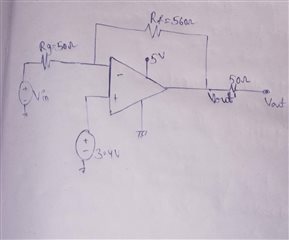
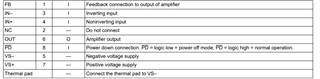
I am working with [OPA858-Q1] and have a question regarding the PDbar (Power Down) pin.

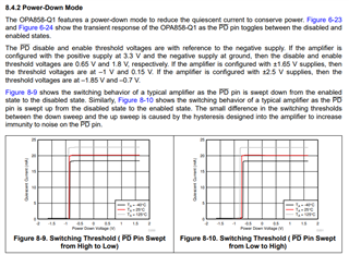
The datasheet mentions that for normal operation, the PDbar pin must be connected to the positive supply. However, under the "Power Down" section, the behavior at ±2.5V supply seems to differ.

  1. What should the PDbar pin be connected to when operating at ±2.5V to enable the op-amp?
  2. Could someone explain the reasoning behind this behavior?
  3. will there be any change in voltage at input inverting terminal if we are giving PDbar to positive supply?

I appreciate any insights or references to clarify this.

Thank you!

  • The behaviour does not differ. Please explain what exactly seems to be different.

    1. +2.5 V

    2. High = enabled, low = powered down.

    3. No (except when there are feedback resistors connecting it to the output).

  • in 3rd point when there is feedback resistor connecting output to input  , how will it change the voltage at inverting input pin of opamp by changing PDbar pin voltage ?

  • When the /PD pin is low, the output is disabled, so no current flows through the feedback resistors. (But the resistors still connect the input to the output load.)

  • Hi Deepthi,

    Clemens is correct, you will not see any voltage changes at the input nodes due to powering the PD pin when enabling the device.

    Best Regards,

    Ignacio

  • then why i have some voltage at inverting terminal(0.1V) , even though i didn't applied input, its open circuit at input side and one feedback resistance of value 1kOHM is there connected to output from feedback, and non inverting terminal is ground  , and output is 0.760V without applying any input . and what i observed is that inverting terminal voltage is changing by changing supply voltages of opamp .

  • Hi Deepthi,

    Could you please share the supplies the device has in this configuration you're highlighting as well as the Rg resistor being used? A schematic or quick drawing of the circuit in question would help to get more clarity exactly how its setup.

    Best Regards,

    Ignacio

  • this is the circuit diagram and without giving Vin also inverting terminal has 0.1V when measured with multimeter.

  • Hi Deepthi,

    Thank you for the drawing. Just to confirm, you mentioned setting the non-inverting input to ground. In this supply configuration, you would be violating your output voltage range as you would expect the output to be ~0V but the output can only go as low as ~1.05V. 

    Best Regards,

    Ignacio

  • thanks for the reply team , actually when i am connecting my non inverting terminal to ground , in that case i am observing 0.1V at the input inverting pin of the opamp ,and in this configuration with common mode volatge Vcm =1V the results are like this 

    where bias current and offset voltages are not matching , and when my feedback resitance is 10Meg with Rg=1Meg with same Vcm =1V the my output stuck at 2.05V and its not changing even though i am varying my input .

  • i tried giving input current directly without giving this resistor Rg and voltage input , in that case also i am not getting the results as expected  its deviated from original value .can you please tell me why i am facing this issue with this opamp sir .

  • Hi Deepthi,

    The results are about what we'd expect as you are running into output limitations. As far as the bias current and offset not matching, is this how you are attempting to capture this data? Capturing .4pA of bias current is extremely difficult and is likely why you are not seeing the result you expect. As for offset voltage, the device datasheet captures and guarantees an offset voltage value in a very specific circuit condition. Deviating from this configuration will result in a different offset voltage. When trying the larger feedback resistor, you could be running into a completely new situation where the device is now unstable. We have seen where a device outputs an erroneous dc signal due to it being unstable. Using such a large value like 10MEG is likely causing this issue you see. 

    Best regards,

    Ignacio

  • i am capturing the data of bias current from SMU ,which can capture upto pA .So, won't it work for high values of feedback resistors? I chose this amplifier specifically to achieve a transimpedance gain of 1 GΩ. Do you have any suggestions on how to use this op-amp effectively in this configuration? can you please help me in this issue team?