This thread has been locked.

If you have a related question, please click the "Ask a related question" button in the top right corner. The newly created question will be automatically linked to this question.

ALM2403-Q1: ALM2403-Q1

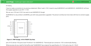
Part Number: ALM2403-Q1
Other Parts Discussed in Thread: OPA547, OPA593, OPA547EVM, OPA593EVM
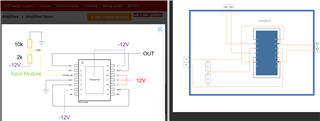
Tool/software:

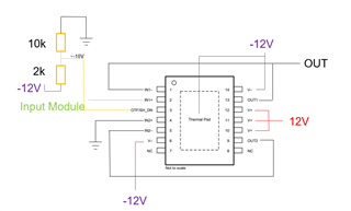
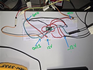
I did purchase ALM2403-Q1  dual-power op amp.

Connections made:

pin 1 : NI FPGA GND

pin2: NI FPGA Analog output ch1

pin10:  +12V 

pin 14: -12V

I am always getting 0V at Pin 13(  OUT CH of Curr Amp CH1).

Please help identify the issue .

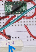
I have mounted the IC on 14 pin IC adaptor.

  • Hi Vishniu,

    Do you have a schematic?

    As is, this is not properly connected. If I were connecting the ALM2403-Q1 to operate as a buffer, I would connect the following pins:

    Pin 1 connected to pin 13

    Pin 2 connected to your input module

    Pin3 connected to a voltage from -10.8V to -6.3V. 

    Pin 6 and  Pin 14 connected to V- (-12V)

    Pin 10, pin 11, pin 12 connected to V+ (12V)

    As you can see, there are many different connections which must be made before you are ready to go. 

    Do you have thermal pad soldered down? You may need this thermal pad to connect to something to dissipate heat during operation. 

    Best,

    Jacob

  • Hello Jacob,

    We had already had an discussion previously before purchasing this OPAMP. Below is the link for the same:

    ALM2402-Q1: ALM2402-Q1 - Amplifiers forum - Amplifiers - TI E2E support forums

    I wanted to use ALM2403-Q1 for current amplification for analog signals from my source(NI FPGA card) .

    I did connection according to above comments .

    Do you have thermal pad soldered down? You may need this thermal pad to connect to something to dissipate heat during operation. 

    - NO I didnt. Is this mandate as I am amplifying analog signals(0-10v) from 4ma to 70mA  .

    If it is mandate , how can i do this ? I had mounted this IC on a 14pin IC adapter.

  • Hi Vishnu, 

    Thanks for linking this thread, I now remember our past conversation. 

    No it is not mandated to solder the thermal pad down, I would just be careful to monitor the surface temperature of the device to ensure this is not excessively hot. 

    I did not mention connecting pin 1(IN-1) to pin 13(OUT1) in my previous  post, but my schematic shows this connection:

    This is required to create the buffer. 

    The other important connection is to the OTF/SHDN pin. This must be at least 1.2V above the V- rail to ensure the device is enabled. It is important to ensure this net does not exceed V- + 5.7V otherwise the device will sustain damage. 

    This voltage can be easily created using a voltage divider between V+ and V-, or we can use an external voltage resource.

    Are you using CH2 of the amplifier for any function?

    If not, it may be a good idea to connect it like a buffer with an input of GND : How to Properly Configure Unused Operational Amplifiers

    Please let me know if you have any questions. 

    Best,

    Jacob

  • Hello Jacob,

    1. Okay I will keep  pin 1(IN-1) to pin 13(OUT1) shorted by default in the IC and then take amplified Analog out from pin 13 . Also pin1(IN1-) should be connected with GND  of  analog source correct? in my case NI FPGA GND.

    2. Pin 3: OTF/SHDN pin

    I have -3.3v , -5v available in my SMPS . Can I source -5v to Pin 3? 

    3. yes I will be using  CH2 of amplifier too .

    Can you summarize me any particular point in connections to be taken care when using both CH's of this Amplifier.   

    Also in case if I am only using CH1 , then I should connect GND to IN2+ {pin 4} . correct?

  • HI Vishnu, 

    No, do not connect pin 1 to GND. this pin only needs to connect to OUT1 (pin13)

    IN1+ can connect to FPGA output,  and the FPGA GND must reference the AGND on your board.

    -5V would be 7V higher than -12V, so this is not allowed. I think a voltage divider is the best option here.

    Correct, if you are only using one channel of the amp, you would connect IN+ to GND and you would connect IN-2 to OUT2.

    Thanks,

    Jacob

  • Hello Jacob,

    OTF/SHDN pin

    Above is the voltage range for OTF/SHDN pin.

    V- is  -12V  so range is [-12-0.2] to [-12 + 5.7] => -12.2V to -6.3V.

    So how about providing -12V itself which is in above range

  • Correct -12V is valid. 

    -12V would put the amp into shutdown mode:

    This table references V- as the DUT has no idea of what true GND is in your system

    This means you need a voltage between -10.8V and -6.3V to enable the DUT

  • okay.

    So voltage in this range  [-10.8V to -6.3V]  should be applied at OTF/SHDN pin.

    So using +12V and -12V, which is 24V, A voltage divider ckt with R1=10Kohm ,R2=2.2Kohm will give me Vout across R2  = -7.68V .

    This is good? pls confirm 

  • Hi Vishnu,

    So voltage in this range  [-10.8V to -6.3V]  should be applied at OTF/SHDN pin.

    Correct

    So using +12V and -12V, which is 24V, A voltage divider ckt with R1=10Kohm ,R2=2.2Kohm will give me Vout across R2  = -7.68V .

    Yes, this is a good voltage value to use. The OTF pin consumes a slight amount of current, but this voltage should leave enough tolerance to allow the amp to remain in operational mode.

    Best,

    Jacob

  • Thanks

    I will test and let you know the feedback

  • Perfect, this should work well after the change.

    Thanks!

    Jacob

  • ALM2403-Q1_CKT_Board Design.pdf

    Request you to Please review this design ! 

    I am getting continuity across V+ and V- in this design which is not expected. Please help analyze what is wrong here. 

    Pin 1 connected to pin 13

    Pin 2 connected to your input module

    Pin3 connected to a voltage -7.68V . 1/4 watt resistors used.

    Pin 6 and  Pin 14 connected to V- (-12V)

    Pin 10, pin 11, pin 12 connected to V+ (12V)

  • Hi Vishnu,

    This is a sound design, good connections at every pin. 

    When you say continuity across V+ to V- you mean you are measuring with a DMM and finding low resistance path between terminals?

    What is the reading at OUT1 when you connect to the pin 2 to GND? 

    Thanks,

    Jacob

  • yes when i do continuity check using DMM across V+ AND V- , I am getting beep sound(they are shorted). Also I could see spark coming and i immediately disconnected power.

  • Spark is no good Disappointed

    I can solder up a device and show that this configuration works. 

    I do not know why this is an issue for your particular setup. 

    Thanks,

    Jacob

  • Ya. Asper design also there should not be a short between V+ and V-  I could see and not even when tested across pin 6 and 10 of the IC alone (without other ckt).

    Confused and debugging!!

    1/4 watt resistors are good? 

  • Yes, thanks for your patience as we work through this problem. 

    I will have time to solder the part to an adapter board like you are using in ~3 hours from now. I can send you over my results when I hook the part up to my test equipment. 

    How is the circuit being ground referenced? Do you have anything which connects to the DGND of the input module? 

    Best,

    Jacob

  • okay. Thanks for your support on this.

    How is the circuit being ground referenced? Do you have anything which connects to the DGND of the input module? 

    - NO. NI FPGA DGND is not connected to any pin of amplifier or CKT

  • Hi Vishnu, 

    Thanks, this is good to know. 

    I will report my test results in the next couple of hours. 

    Best,

    Jacob

  • HI Vishnu, 

    I connected my circuit exactly as you have in your schematic, and I do not have problems with my circuit operation.

    Perhaps it is necessary to start over with a fresh unit.

    Also, if it is possible, I would try to place some .1uF decoupling capacitors close to the VCC and VEE pins of the device. This can help reject some of the HF noise which would otherwise couple into the device supply pins.  

    Thanks,

    Jacob

  • Hello Jacob,

    I did make the circuit freshly . No I dont have short between V+ and V- .

    Observations//

    1. 24V measured across V+,V-  // Expected.

    2. 11.5V measured across IN1+ and common GND(GND of PS) . // Not expected

    3. 11.5V measured across Out1 and common GND(GND of PS) . // Not expected

    After I connect my source Analog out signal (0-5v) at IN1+ also same 11.5v was measured at IN1+ and OUT1 aswell .

    Please help debug what might be wrong here!!

  • Hi Vishnu,

    Good to hear that the short is fixed.

    It is strange to hear that the IN+ is set to 11.5V.

    Could you try connecting this pin to the PSU common GND?

    What is SHDN voltage measured under the following two conditions:

    voltage between SHDN and V-

    voltage between SHDN and PSU common

    Best,

    Jacob

  • voltage between SHDN and V- // 22.2V

    voltage between SHDN and PSU common // 10.9V

    Could you try connecting this pin to the PSU common GND? //  Which pin I should try connecting to PSU Common GND?

  • Connect IN+1 to GND common. 

    Thanks,

    Jacob

  • IN1+ is where I will connect Source AO signal , so I should not connect both  

  • Hi Vishnu, correct, we cannot connect both at the same time. 

    I am concerned why the voltage between SHDN and V- is 22.2V. This would mean we are at 22.2V-12V = 10.2V relative to GND or about 10.9V as you measure.

    We should be at V- +5.7V at most. Weren't we targeting to be at something like -7.68V relative to GND?

    Thanks,

    Jacob

  • So I connected PSU GND to IN+1 .

    voltage between SHDN and V- // 22.2V

    voltage between SHDN and PSU common // 8.2V

    Weren't we targeting to be at something like -7.68V relative to GND?

    yes

  • Hi Vishnu, 

    Did we get the resistor divider backwards?

    Technically this OTF/SHDN voltage is currently damaging the device. In fact, it may be likely that this voltage has damaged the device to a point where it will not operate correctly now. I had success with the 10k and 2.21kohm resistor for setting the OTF/SHDN pin voltage. 

    Can we swap some of the resistive components around to fix this voltage setting?

    Thanks,

    Jacob

  • Before applying 12V+,12V- Voltage to CKT, I verified:

     1. Resistor across pin3 and V- as 2.2kohm and across pin3 and V+ as 10kohm . 

    2. No shorting between :

    V+,V- 

    IN1+,IN2+

    Out1,Out2

    3. Continuity check also verified to confirm the implementation asper the ckt board design .

    After applying the power ,12V+,12V- Voltage to CKT, I verified:

    1. There is shorting between V+,V-

    2. Pin 14 is shorted to pin 10,11,12 and V+

    *NOTE:  I removed IC from Ckt board and then checked  if these pins are still shorted within the IC and yes it was shorted .

    This means after applying power to  IC, IC  had damaged which had resulted in this shorting within IC .

    I experimented with 2 of my IC's and both are damaged now . The IC is very sensitive or not sure why this is happening .

  • TI OPA547T //

    How about this Amplifier? Can this be used for same application? 

    Would this be better as "ALM2403-Q1" IC is very much sensitive I feel

  • Hi Vishnu, 

    Sorry to hear that you are still encountering trouble. 

    I am not sure why this would be the case. ALM2403-Q1 is actually pretty strong when it comes to overstress tolerance and ESD. 

    Yes, you can use OPA547 as well. This device is physically larger and higher cost:


    Why not use something like OPA593? This would be a smaller package, lower cost, and better performance. 

    We also have an EVM available for both devices OPA547EVM and OPA593EVM.

    I know ALM2403-Q1 is a perfectly fine device for this application, I suspect that either the SHDN voltage is too high, or some similar overstress damage is occurring. I was able to see the device operate on my 14 pin TSSOP adapter board without any issue. 

    The shorting confirms that large damage occurred within the device.

    In our last test, we observed that the SHDN pin voltage was about 14V above abs max. this is likely what damaged the device. 

    Thanks,

    Jacob

    Best,

    Jacob

  • Hi Jacob,

    I am not sure why this would be the case. ALM2403-Q1 is actually pretty strong when it comes to overstress tolerance and ESD.

    -> Not sure as the ckt design is verified from your side and we connected it same way. Else can you again revisit the CKT diagram shared or provide your own ckt diagram from scratch to freshly approach this ?

    EVAL Boards are not preferred due to higher price .  

    Considering OPA593, What are the things to be taken care in electrical connection to use it for our application? 

  • -> Not sure as the ckt design is verified from your side and we connected it same way. Else can you again revisit the CKT diagram shared or provide your own ckt diagram from scratch to freshly approach this ?

    EVAL Boards are not preferred due to higher price . 

    Are you designing your own board to interface the power amp with your source AO? EVM would just be used for lab testing, and the custom board you design would be much cheaper and smaller. 

    OPA593 is reasonably similar to ALM203-Q1 from an implementation standpoint.

    Best,

    Jacob

  • Design comparison

    The Design you had provided and the previous design are attached here.

    In old design V+ =12v , V- = -12V and voltage across 2.2kohm with reference to V- (-12v) was passed to pin 3 .

    In the new design you have provided, Voltage across 10kohm with reference to 0V  is passed to pin3.

    Above is one key differance I observed.

    The GND reference you mentioned in new design, at IN2+ and at 10Kohm resistance  should be Source AO channel GND ?

  • HI Vishnu, 

    Correct, I made a few small changes. 

    There are some advantages to the first design, but I figured there is slightly more risk in using V+ and V- in a voltage divider in the event that the V+ rail ramps faster than the V- rail. This new design should help prevent positive voltages from appearing at the SHDN pin. 

    The GND reference you mentioned in new design, at IN2+ and at 10Kohm resistance  should be Source AO channel GND ?

    Yes, this should be source AO GND which is also the same as PSU common GND. 

    I also connect thermal pad to V-, but this can also be electrically floating if desired.

    Thanks,

    Jacob

  • Hello Jacob,

    I did connections asper your new design . I didn't get any pin short here which is good but the voltage out is not as expected.

    Below I will provide the voltage observed at Out1+ with respect to Voltage provided at IN1+ ;

    IN1+   Out1+

    1v -     0.110
    2v-     1.10
    3v-     2.10
    4v-     3.09
    5v-     4.09

    0.0v-   -0.835
    0.1v-   -0.76
    0.2v-   -0.68
    0.5v-   -0.38
    0.8v-   -0.081
    0.9v-   0.018

    Out1+ voltage is measured across Out1(pin13) and Common GND.

    Please analyze and provide solutions

  • Hey Vishnu, 

    Thanks for taking this data, it is interesting to see.

    We are running out of options here for debug, but i am determined to get this circuit working. I built the exact circuit we had originally with no issue. My new revision of the circuit is very similar, so I would expect this to work as well. 

    I find it interesting that the OUT+ is off by .9V consistently. This is very strange. I have seen cases like this where the op amp self powers through the ESD diode path https://e2e.ti.com/blogs_/archives/b/precisionhub/posts/the-self-powering-device. It might be worthwhile to probe pins 10-12 relative to GND. 

    Can you take a picture of your board? I want to make sure everything is correct.

    Are you able to measure the current flowing into the supply rails of the device? This can tell us what the device is trying to do. 

    Thanks,

    Jacob

  • Voltage across pin3 and GND is  -9.45V

    CKT board snap attached.

    The power source is an SMPS , and so cant measure the current draw by the ckt .

  • Vishnu, 

    Thanks for the picture,

    I can see the problem (I think)

    It looks like pins 10 and pins 12 are not connected to V+

    These all need to connect to V+. I only see one wire

    Thanks,

    Jacob

  • Pin 10,11,12 are internally shorted within IC , hence only pin12 was connected to V+

  • Hi Vishnu,

    I believe this is the case, but it appears that the output stage is not using any drive voltage. 

    For fun, could you connect these pins to 12V?

    Thanks,

    Jacob

  • Vishnu, 

    If this does not solve the problem, then the 12V rail may not be functioning, or the device may not be making connection with 12V rail. 

    Thanks,

    Jacob

  • Hello Jacob,

    I did connect pin 10,11,12 to V+ and the circuit is functional now .

    The output is inline with the IN1+ voltage provided. 

    But there in an increasing deviation in the voltage measured at OUT1 wrt IN1+ as we increase voltage say (IN1+ = 0.1v TO 5V) .

    I have captured the observation in word file attached.

    #NOTE:

    In the screenshots attached please note : I have integrated Current amplification module for only FLOCK signal and its associated SW variable read is  "Appl_Flock_Asil_buffer.Volt". Refer .jpg file attached.  Curr_amplifier test.docx

    Is there anything we can do for reducing this deviation ?

  • Hey Vishnu, 

    Some error will come from the breadboard, this is non-ideal layout for the device. 

    What is reading this output voltage?

    It looks like .8V setting is getting readback of .760V

    It looks like 4.997V setting is getting readback at 4.835V, correct?

    It may be necessary to put a low pass filter before your ADC is you are trying to readback accurate voltage. 

    Have you confirmed that the actual output voltage is accurate relative to what your software is reporting?

    Thanks,

    Jacob

  • This deviation is accepteble for our test currently. In case requirement changes  a low pass filter I will add .

    Thankyou very much for your consistent support on this project. 

  • Hey Vishnu, 

    Happy to help!

    Great to hear that this design is suitable. Please reach out if any other questions come up.

    Thanks,

    Jacob