This thread has been locked.

If you have a related question, please click the "Ask a related question" button in the top right corner. The newly created question will be automatically linked to this question.

INA597: Offset Issue

Part Number: INA597
Other Parts Discussed in Thread: MSP430FR2676

Tool/software:

Good Day,

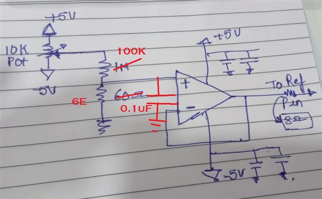
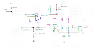
We have developed a INA597 based high side current measurement circuit. After INA597 there are 8 stages of amplifications. Because of the high gain at the last stages of amplification even the nominal offset of the INA causes saturation of the last stages.

We have tried out different offset techniques but the last attempt we are only able to zero the offset temporarily.

We could share further details in a one to one correspondence. 

Looking forward to a positive response from your end.

Kind Regards,

Aditya Ayachit

  • Hello Aditya,

    If you would like to send me a schematic directly, I have sent you a friend request. Could you share the schematic, as well as the description of the input with the amount of current you are trying to measure and what the desired output range is?

    Best,
    Gerasimos

  • Hello Aditya,

    Just wanted to follow up here. Do you still need assistance with your circuit?

    Best,
    Gerasimos

  • Hello Gerasimos,

    We definitely require your help. 

    ---------------------

    The background:

    ---------------------

    We want to develop a circuit for conducting Ageing test/ Burn-in test for electronic locks.

    Essentially the locks operate in 2 modes: Active mode and sleep mode.

    After manufacturing and before dispatch each lock undergoes this test.

    The sleep current of the lock depending on the model is 15 to 100uA.

    The active current is in the range of 400mA to 1.5A

    We have selected the method of high side current measurement. Though it is difficult to implement as compared to low side we believe that it has certain benefits which tilt the scale in it's favor.

    The final PCB has the analog circuit + MSP430FR2676 + LCD + 3 keys.

    But currently we are working only on the analog circuit.

    ------------------------

    Circuit Description

    ------------------------

    (Refer Ageing_Micro_Schematic.pdf)

    The Positive terminal of the unit under test is connected to J1-1.

    The negative terminal is connected to J1-2.

    The load current for the circuit goes through the resistance of approx. 0.363 ohm (R1-R11 in parallel).

    This generates differential voltage at HP and LP points.

    This is the input to INA597.

    Rest of the circuit is quite straight forward. 8 low offset op-amps (OPAx191) are connected in daisy chain.

    Our assumption here is that because the offset voltages are small the later stages should not get saturated.

    But it is seen that with INA597 reference pin connected to ground , the 5th stage on-wards are saturated.

    We also tried out the dcl_ageing_v01_310325-2025-06-18T06-42.zip

    We had simulated the circuit in "PSpice for TI" earlier. We will try and attach the appropriate file if possible.

    Another attempt was made to compensate the offset by adding a circuit to the reference pin.

    It does trim the voltage at the 5th to 8th Stage but the voltage does not remain constant and steadily climbs to saturation.

    There could be possibly some points which I have not clarified properly or glossed over. Please let me know if you would need further clarifications on those points and I will share them.

    Looking forward for your support.

    Kind Regards,

    Aditya Ayachit

    Circuit_calculations.xlsxAgeing_Micro_Schematic.pdf 

  • Hey Aditya,

    15uA to 1.5A is a large amount of dynamic range (5 decades), and I believe that it may benefit you to have multiple signal paths with multiple shunt resistances, especially since you have two discrete ranges of current to sense. If you are able to know when the device is in active and sleep mode, you can use this to switch between the two networks/signal paths, but you may now size your resistor appropriately for the tolerable amount of voltage drop, as well as remove the need for such high gain. If you are unable to know which state you are in and cannot digitally set your shunt path, you may be able to implement a clip detection circuit to switch between the large and small shunt.

    Having a gain of 68.9k on a 5V supply approaches the physical limit of how good offset voltage can get, and it is exceedingly rare to find a difference amplifier with sufficient offset voltage to be able to sustain a downstream gain of 68.9k without saturating. Increasing the value of shunt resistance for your lower current values will give you a larger input voltage

    Ultimately the best bet is to have your gain in the front end, and the closest to the front end that you can get is the shunt resistance. Because you have two distinct states you want to measure, two signal paths make sense here.

    Best,
    Gerasimos

  • Dear Gerasimos,

    Thank you for your response. We will take the required actions accordingly. If I want to switch in/out the shunt resistors, do you have any suggestions?

    Appreciating your help greatly.

    Kind Regards,

    Aditya Ayachit

  • Hey Aditya

    Are you able to know when your downstream device is in sleep mode and active mode, or will you need to sense this based on consumed current?

    Best,
    Gerasimos

  • Hello Gerasimos,

    I am sure that I have replied to you earlier, but I don't see it here. But essentially I am not able to detect if the device is in sleep mode or active mode. There are different models of locks and each model will have different duration. 

    Looking forward to your reply.

    Kind Regards,

    Aditya Ayachit

  • Hello Aditya,

    You may be able to accomplish something like this with a saturation detection circuit. I will create a mockup, but the final values should be determined on your end.

    I will need a day or so to make a functional circuit that behaves appropriately, I will provide an update by EoD tomorrow.

    Best,
    Gerasimos

  • Hello Gerasimos,

    I will look forward to your response. We will calculate the final values.

    Kind Regards,

    Aditya Ayachit

  • Hey Aditya,

    I am having some trouble with the comparator implementation, I have reached out to the comparator team here: https://e2e.ti.com/support/amplifiers-group/amplifiers/f/amplifiers-forum/1535463/tlv1862-saturation-detection-current-sense

    However, once the front-end is created, I can work on the downstream shunt sense.

    Best,
    Gerasimos

  • Hello Aditya,

    Here is a proof of concept design to switch between two different shunts. The goal here is as follows. VCVS1 is an ideal approximation of a difference amplifier, INA597 may be added here. The voltage controlled switch can be substituted with a FET.

    1. When the voltage across the shunt resistor exceeds a certain threshold, the comparator triggers to add a smaller resistor in parallel, giving a different lower shunt gain for high current measurement.
    2. This comparator has a large amount of hysteresis, and will not return to the low current range until the output starts to drop below a certain threshold
    3. Care must be taken when selecting shunt resistor values, I would still target shunts that are several orders of magnitude smaller than the feedback and input resistances of INA597.
    4. The 2nd VCVS is just there for monitoring purposes and can be excluded.

    Best,
    Gerasimos