This thread has been locked.

If you have a related question, please click the "Ask a related question" button in the top right corner. The newly created question will be automatically linked to this question.

OPA847: PCB design questions my transimpedance amplifier

Part Number: OPA847
Other Parts Discussed in Thread: OPA855

Tool/software:

Hello,

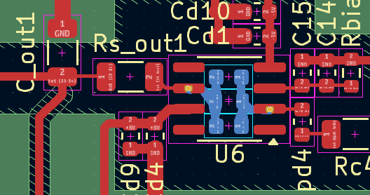
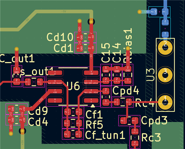
I’m currently working on a 4-layer PCB for a transimpedance amplifier design, and I’m looking for resources and feedback on best practices.

I’ve already reviewed some documentation on the topic, but I still have a few open questions:

  1. Regarding the copper-free areas around the amplifier:

    • What is the recommended clearance distance?

    • Should the ±5 V decoupling capacitors be placed inside or outside this area? (Inside keeps them close to the amplifier, but outside respects the guard zone while increasing the distance from the inputs).

  2. For the feedback components (resistors and capacitors):

    • Is it better to keep them on the same layer as the amplifier, even if that means placing them slightly farther away,

    • or to use via-in-pad (In–, Vout) and mount them directly on the opposite side?

  3. Regarding via stitching:

    • At what stage should it be added to the layout?

    • What are the recommended rules for placing vias around the amplifier and sensitive areas?

  4. My design also includes a 400 V high-voltage supply for the APD. What would be the best practices to properly isolate this HV section from the TIA, in order to minimize coupling while ensuring both safety and analog performance?

Finally, I’d greatly appreciate a general review of my PCB design, highlighting any critical points or potential mistakes I should be aware of.

Thanks !

  • Hello Joe,

      I apologize for the delay on a reply to your thread. You already did pretty good research on this topic.

    1. We recommend inner layer plane cutoff for any power/ground plane coverage under important signal traces. It should be enough clearance to cover the signal trace, therefore, no need to clear all around the amplifier.
      1. For example, from the OPA855 datasheet and OPA85x EVM:

        The white region is showing the inner plane layer cutoff (copper-free) region only for the feedback trace. I would maybe recommend extending it a bit to the trace from PD to inverting pin of the amplifier as well. And, we usually do this to the trace to the load resistor as well which is not shown in first picture, but shown in second picture.
      2. Therefore, decoupling capacitor priority is to be placed as close to the supply pins as possible, and no need to cut the region to these capacitors. It is actually recommended to have a power/ground plane to these capacitors to increase the path to the supply and ground connections (enhance low-impedance path) by using vias around these capacitors to the inner ground/power planes and any coverage on top/bottom layers as well. Also, planes allow for many different current return path under or over any trace above or below the plane (this helps avoid ground loops). 

    2. This one is a bit difficult to answer. It really depends on how far away these components will be. Most likely keeping the feedback resistor/capacitor on the same top layer as the amplifier is best. And, then try to find a path for shortest trace to the amplifier feedback/out/input pins. Decoupling capacitors to supply power pins of the amplifier can be placed on the bottom layer of your PCB. 

    3. We usually do the vias last, and we avoid using vias for signal paths. Via stitching can be done around the input and output traces to create a shield around these important paths. It is also done around the decoupling capacitors and ground connections as explained in #1 

    4. That is a good point to separate PD supplies from the rest of the board. It is recommended to separate the region of GND and supply to this PD. This should be pretty easy to do since it will only be on one region of the board. I haven't dealt with these very high voltages before, but I read that you need to add slot cuts to make sure you avoid arcing and creepage and would make sure the PCB material used can handle up to these voltages.

      I am going to link a couple resources I have found very helpful. It is a lot of information, but would recommend reading through them and let us know if you have any questions or clarifications:

    1.  LMH6629: High-Speed Transimpedance Amplifier for Single-Photon Detection 
    2.  OPA855-Q1: Output layout instruction 
    3.  https://www.ti.com/lit/ml/slyp173/slyp173.pdf
    4.  https://www.ti.com/lit/ml/slup419/slup419.pdf?

    Thank you!
    Sima