This thread has been locked.

If you have a related question, please click the "Ask a related question" button in the top right corner. The newly created question will be automatically linked to this question.

LMH6629: High-Speed Transimpedance Amplifier for Single-Photon Detection

Part Number: LMH6629
Other Parts Discussed in Thread: OPA855, OPA858

I’m trying to use LMH6629 for single-photon detection from a Hamamtsu S13360 MPPC

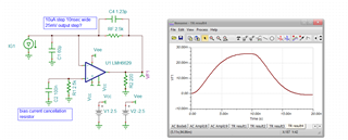
The pulses of current from the MPPC are small and fast.  I believe they’re in the 10µA range and last 10ns, depending on the impedance of the input. 


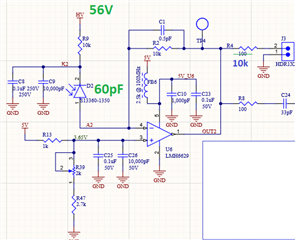
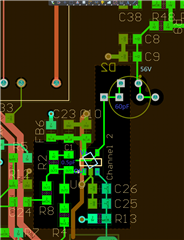
I had problems with the amplifier oscillating in the 700 MHz range.  Increasing the feedback capacitor (C1) made the oscillation worse.  I removed the ground under the part and around the MPPC anode trace (A2).  This helped, but I have had to place a 1000pF decoupling cap on top of the LMH6629 to reduce ringing.

It’s working well now, but here are goals I still have for it:

  • Increase stability – Is there a way to inject a signal to measure phase margin?  I want to know it won't oscillate if the MPPC's capacitance is a little higher.
  • Higher high-frequency gain

In my application I only care about counting the number of photons. I do not need to know the time they arrive.  

  • Hello Charles,

      Removing the ground plane was a good solution fix. For the additional decoupling cap, was the placed on top of C10? 

      Looking at MPPC datasheet, it does seem like a pretty fast rise time with a relatively larger capacitance of 60pF. 

      With the LMH6629, the below calculation is the resultant closed-loop bandwidth and feedback capacitance at Q = 0.707 (minimal peaking at phase margin around 65 degrees):

      As you have tested out, increasing the feedback capacitance will lower bandwidth but should have increased stability. Decreasing feedback capacitance will decrease phase margin, and increase bandwidth (aiming for 45 degrees of phase margin for stability). 

      For the listed goals, I would suggest moving the diode (D2) as close as possible to the input of the amplifier which will increase overall stability. And, if it fits your other design requirements, I would also suggest trying out the OPA855. This is our high bandwidth amplifier, TIA calculation below:

      For even higher gain designs, we usually suggest adding a low noise second stage.

      Overall, your layout is pretty clean but if you would like to review more suggestions, Kai has written up a very useful guide on layout for TIAs with details on parasitic inductance and capacitance at this e2e thread

      Also, here is an e2e thread showing various variations of stability simulations for TIAs. Please feel free to ask further questions on the linked e2e threads. 

    Thank you,

    Sima 

  • This is very helpful.  I recommend anyone facing similar issues follow the link's in 's response.

  • Well that 40MHz BW is not going to reproduce a 10nsec pulse very well - here is a simplified sim where I did add a bias current cancellation R on the V+ input, you might want to do the same in your circuit to get the 0 input current output V closer to your target. If you are just trying to trigger a comparator for pulse event, this may be enough. If you need more BW, there is a newer faster part, OPA855. You can always increas Zt bandwidth reducing your target gain and adding a postamplifier if need be. 

    For instance if I redesign for gain of 2.5kohm, I get this pulse, 

  • Might as well do some more with that 2.5kohm setting, 

    Here is a longer time showing slight undershoot, 

    And the frequency response, I had targeted a Q=0.63, 75MHz F-3dB

    And this file, 

    LMH6629 sim for transimpedance.TSC

  • Thanks for this info. I don't really know the pulse duration associated with an MPPC avalanche event.  I think when a photo hits it (or in avalanche events associated with dark noise) you get a million electrons flowing over a very brief period.

    I tried to break the loop and analyze my circuit.

    My 1/Beta shows a phase of 180 at DC.  

    What am I doing wrong?  Here is my TSC file: 

    /cfs-file/__key/communityserver-discussions-components-files/14/LMH6629OL.TSC

  • You need to use a meter and reverse it to get 0deg at DC. On the Vfb point, 

    incidentally, this technique is slightly less desirable than the one shown in this article, 

    the approach you show isolates the open loop output impedance from the feedback network - also try to include your load, 

    https://www.planetanalog.com/stability-issues-for-high-speed-amplifiers-introductory-background-and-improved-analysis-insight-5/

    My sims show stability incidentally, but a load would be nice to have. 

  • Hello Charles,

      Were you able to confirm the stability? Another way to view your above snippet, would be to look at how much the phase has shifted from its initial point of -180 degrees. It would relative to that value instead of the usual 180 degrees.

    Thank you,

    Sima 

  • Were you able to confirm the stability? Another way to view your above snippet, would be to look at how much the phase has shifted from its initial point of -180 degrees. It would relative to that value instead of the usual 180 degrees.

    I am not completely sure of this approach of breaking the loop in the case of my circuit where in closed-loop it is a transimpedance amplifier.

    Here's what I get:

    I have run the simulation varying the unwanted C10, which is the capacitance of my photodiode plus the traces. I have also varying C1 and R1.  C10 seems to cause a dip on phase in the MHz range.  Increasing C1 decreases the unity gain frequency, as expected.  

    I have a very unclear understanding of what this means for stability.  Here's what I know from experimentation in the lab with the actual part:

    • Capacitance at the input, represented by C10, is bad.  If I have too much ground around the input it oscillates intermittently with strong spectrual components in the 100s of MHz.  
    • If I remove the ground from the input and just have the 60pF MPPC photodiode there, it's stable iff C1 > 0.5pF.  The 0.5pF makes a huge difference.
    • Increasing R1 doesn't noticably increase stability.  It does increase gain, but the pulses I'm amplifying are fast, so going from 10k to 100k maybe doubles the amplitude of the pulses at the output.  

    I have had better results doing transient analysis with the loop closed as in the actual circuit.

    I can see from the transient analsys that things that would reduce stability cause it to overshoot or ring.  Am I correct that the absence of ringing in transient analysis is a sign of stability but not as conclusive as open-loop AC analysis?

  • Hi Charles,

    I would perform the phase stability analysis this way:

    charles_lmh6629.TSC

    But I think the issue here is the layout! Am I right that the ground plane is largely removed under the LMH6629 circuit and that pin 2 of OPA858 is not directly connected to the solid ground plane but sees signal ground only via the brown copper trace?

    There's no need to remove the ground plane under C26, C25 and R13. Also, C10, C23, C25 and C26 should each have vias at their ground terminals directly going to the solid ground plane. Remove the solid ground plane under FB6, though.

    And D2 as well as the ground connections of C8 and C9 are too far away from the OPA858. Keep in mind that every single millimeter counts!

    Kai

  • Thanks for this response.  

    Am I right that the ground plane is largely removed under the LMH6629 circuit and that pin 2 of OPA858 is not directly connected to the solid ground plane but sees signal ground only via the brown copper trace? There's no need to remove the ground plane under C26, C25 and R13.

    I started out with a copper pour around the trace going to the inverting node (Pin 4).  This was a bad idea.

    So then I went the other direction, and as you notice, the ground is no longer connected to a solid ground plane.  I think the 1000pF decoupling cap I have soldered on top of the part is mitigating this problem.  You have a very good point that I need to keep ground way from the interverting node but no from the bias network on the non-inverting node.  What about removing ground from under the output?  I think I'm going to replace the ground place under the left side of the part.  Do you think this output capacitance will be a problem?  

    I'm going to try these layout changes.  I'm hoping replacing the ground plane under the part eliminates the need for a decoupling cap soldered right over the part.  

  • Hi Charles,

    I would use such a layout:

    Above you see the top layer with the components. The photodetector is shown at the right of LMH6629, connecting to pin 4. I hope you do not use a cable to connect the photodetector to the TIA??

    Please note that all components that have to be connected to the LMH6629 do this with the shortest connections possible. This means the decoupling caps at pin 5, the feedback resistor and the feedback capacitance between pin 1 and pin 4, the output isolation resistor at pin 1, the bias voltage decoupling cap at pin 3 and the photodetector at pin 4. This is how the LMH6629 is expected to be wired.

    The two decoupling caps should be fully identical. Otherwise you risk a nasty resonance. The same is true for the decoupling cap at pin 3 and the decoupling cap at the cathode of photodetector. Use only one decoupling cap with ultra small package (0603 or 0402). If you need more decoupling capacitance, then only use (two) identical caps in parallel.

    Note how I have placed vias at all the ground terminals. There are always three vias close together to minimize the inductance to the ground plane.

    Also note the many vias I have placed all over the printed circuit board. (Here only the closest ground vias arround the components of TIA are shown. Many more vias have to be added farer away.)

    Also note where exactly I have removed the ground plane in the top layer under the series components of low pass filters and also below the feedback components and the output isolation resistor:

    In the next picture you see the ground removes in the second layer (inner layer below the top layer):

    The ground removes may be repeated in the third layer and bottom layer of a 4-layer board. But really essential are the ground removes in the second layer just below the top layer (140µm in a typical 4-layer board).

    In my circuits I use a solid ground plane in the bottom layer without any ground removes, because I need the soild ground plane in the bottom layer as a shield. This usually presents no issues referring to stray capacitance, because the bottom layer is more than ten times away from the top layer (1500µm) than the second layer is (140µm).

    Kai

  • Thanks for these detailed layout diagrams.

    The two decoupling caps should be fully identical. Otherwise you risk a nasty resonance. The same is true for the decoupling cap at pin 3 and the decoupling cap at the cathode of photodetector.

    This goes against the folklore that you use caps at least an order of magnitude apart in value to cover high and low frequencies.  

  • Hi Charles,

    This goes against the folklore that you use caps at least an order of magnitude apart in value to cover high and low frequencies. 

    This outdated method still makes sense when you take a SMD tantal cap in a bigger package with higher inductance and noticable ESR in parallel with a SMD ceramic cap in a tiny package with low inductance and low ESR. But today ceramic high caps (X7R) are avaliable which do both, offering a huge capacitance in a tiny package with very low inductance:

    1 ceramic high cap = 1 tantal cap // 1 ceramic cap

    But take care, paralleling two uneven ceramic caps coming in a package with low inductance and low ESR may result in unwanted resonances (-> "Antiresonance"). Then -if you need to parallel decoupling caps at all- you only should parallel identical caps. See figure 8 of this link:

    https://www.signalintegrityjournal.com/articles/1589-the-myth-of-three-capacitor-values

    Or see figure 3-12 from this Murata's appnote:

    c39e.pdf

    Kai

  • , what is the reason for connecting the decoupling caps to ground with a via and connecting the feedback path without a via.  You have to use a via on one or the other, although we want them both as short as possible.  I'm interested in your reasoning for making the feedback path the shortest.

  • Hi Charles,

    what is the reason for connecting the decoupling caps to ground with a via and connecting the feedback path without a via.

    I didn't say that feedback components must not be put on the bottom plane being connected by vias to the top plane. In the following example layout I even use this technique:

    https://e2e.ti.com/support/amplifiers-group/amplifiers/f/amplifiers-forum/1033505/opa847-in-this-tia-circuit-can-i-use-series-resistors-dividing-voltages-to-couple--vbias-to-the-pin-s-anode-when-the-dc-voltage-source-is--5v-and-the-anode-voltage-needs-to-be-1v

    Vias inevitably increase the lengths of wiring because they connect from the top plane to the bottom plane and vice versa. So each via adds 1...1.5nH of unwanted parasitic inductance. For connecting a decoupling cap to a solid ground plane using three or more vias directly at the ground terminal in parallel can considerably decrease the unwanted parasitic inductance. They even profit from the many other vias in the ground fills on the top layer which are a bit farer away from the ground terminal of decoupling cap. See the example layout above. But when having the feedback components on the back side of PCB you can use only very few vias per connection, in most cases only one. Depending on the used OPAmp this may cause stability issues.

    Also, soldering components on both sides of a PCB can considerable increase the costs.

    Kai