LF353: Transimpedance circuit design

Part Number: LF353
Other Parts Discussed in Thread: OPA991, TLV888

Hello, I am designing a transimpedance circuit, which will receive a current between the intervals of 0 - 30mA. This current comes from one of the electrodes that I am using to measure conductivity, the system has been parameterized to measure conductivities from 0 to 9 mS. Making all the adjustments I have generated an excitation signal towards the electrodes of +/- 10 V square wave at a frequency of 5 kHz .... I have already made certain measurements and I have obtained the current range of 0 - 30mA (Bipolar square wave of 5 kHz, 50% duty cycle) Now the next step is that I want to convert this current signal into a voltage signal of +/- 3.5V bipolar square. I have calculated the Transimpedance resistance which has given me 116 Ohm and I have put a 10nF capacitor in parallel. As an amplifier I have used the LF353, but I am not getting good results. I've actually implemented the attached circuit, but I notice that when the conductivity is 9 mS (measured with a commercial meter), the amplifier overheats, distorts the waveform, and clips on the negative side. I'd like to know if this amplifier is suitable for this application, and if not, which one you recommend. I've attached some images of the schematic and the waveform generated at the output of the transimpedance amplifier.


image.png


image.png


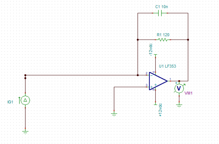
This is the graph when the current passing through the electrodes is approximately +/- 30 mA. The graph represents the output of the transimpedance amplifier. The negative side should be -3.5 V, but it isn't. I'm powering the op amp with +/- 12 V.

I hope you can help me select the op amp if it's incorrectly selected.


Alvaro Tasco

  • Alvaro,

    1. One potential issue is the output current limitations of the op amp, and power dissipation of the op amp.
      1. The vast majority of op amps have an internal current limit.  The LF353 does have an internal current limit (called short circuit limit), but the value is not specified.  The specifications for this device are limited because it is a very old device ( introduced in 1987).  The short circuit limit (Isc), can be quite different across different device models.  For a typical device like LF353, Isc could range from 10mA to 40mA.  Also, the value will change over temperature.  Generally you do not want to drive currents near the short circuit limit with the op amp.  The limit is built in to protect the device from damage.  Power op amps can have much higher short circuit limits.  I think you are likely approaching or exceeding the short circuit limit of the LF353.  Although a power op amp or an op amp with high rated Isc could work for your application, I think there is a better approach (details later).
      2. The power consumption on the op amp will be very high relative to what is expected for this kind of op amp.  This is why your amplifier is overheating.  With a ±12V supply and 30mA of current flowing you will get an output voltage of 30mA*120Ω = 3.6V.  With a 12V supply, the voltage on the internal pull-up transistor is 12V - 3.6V = 8.4V.  This will produce 8.4V*30mA = 252mW of power dissipation.  To calculate the self heating you need theta-JA.  theta-JA = 106.6C/W for this device.  This translates into a 106.6C/W*252mW = 27C.  This means that if ambient temperature is 25C the die temperature would be 27C+25C = 52C.  This is actually surprisingly low, and I suspect it would actually be at a higher temperature.  In any case, there will be some significant self heating.
    2. Another potential problem is stability.  The very large overshoot in your scope waveform makes me think this is an issue. Stability issues can happen because of capacitive load on the output of the op amp, or capacitance on the inverting input.  If your current source input has significant capacitance the 10nF feedback in series with the input capacitance can constitute a capacitive load.  Do you have a model for your electrode?
    3. Most transimpedance amplifiers are amplifying very low current levels (e.g. picoamps from a photodiode).  Op amps transimpedance amplifiers work well for amplifying these low level signals.  When the current levels are much larger, a difference amplifier approach or an instrument amplifier approach is used.  This type of design uses a shunt resistors to translate the current into a voltage.  The shunt could be your 120 ohm resistor in this case, but you could use a smaller resistor to reduce the power dissipation.  This design keeps all the power dissipation in the resistor, so the op amp will not heat up.  Below are some examples of how you could do this.
      1. The "Low side shunt" is the simplest circuit.  This will have some error due to ground resistance and inductance.  The smaller the shunt resistance is the larger the error will become.  For a 50 ohm shunt or 120 ohm shunt, this error will be pretty small.
      2. The "difference amplifier" is normally more accurate than the low side shunt as it senses both sides of the shunt resistor.  In your case though I am not sure this circuit is much better because your shunt resistor can be relatively large.  This circuit does have a loading effect because the input resistor network provides a path for current to flow.  You can make these resistors larger to reduce this error.  When the shunt resistor is small incomparson to the feedback network the error will be small.
      3. The instrumentation amplifier has high input impedance.  Usually this will be the most accurate solution.  However, you have the make sure you do not violate the common mode range.  Usually this will be a more expensive solution.
      4. I think based on your initial selection of LF353 you probably should choose the low side shunt.
    4. Aside from the issues listed above, I would look towards a modern amplifier.  You could use LF353 for the low side monitor if you like, but there are many new devices at low cost that have better specification than LF353. 

    I hope that helps.

    Art

  • Hello Art Kay, first of all thank you very much for taking the time to give your observations which are very valuable for what I am implementing (I will surely do what you say).

    But I want to share what I have been doing, I have reduced the excitation voltage that I apply to the electrodes from +/- 10V (square wave at 5khz) to a voltage level of +/- 5v (square wave at 5 khz) in this way the maximum current generated for a conductivity of approximately 9mS is 13mA. That current is what I am passing through the transimpedance circuit and it clearly improves a lot, in the same way I am not clear that this current of 13mA is within the range of LF353 in the datasheet I cannot find that information and if it is, I do not know what it is jeje.

    Well, I am going to share the voltage signal that the output of the transimpedance circuit gives me, which is very similar to the one obtained theoretically Fig 1. The only thing that causes me curiosity are the peaks that are generated on the edges both rising and falling, I do not know if some parasitic capacitance is affecting and added to the cables and the protoboard these peaks are generated and that may be the cause of a slight heating of the op amp.

    Together with the resistance of Rf = 116Ohm, I am using a 10nF capacitor that gives me approximately an Fc = 137Khz, but in reality I do not see changes in the waveform, experimentally I have changed the capacitor some in the order of microfarad but I only notice that the waveform changes and the LF353 tends to heat up a little more, but I do not see any improvement in the peaks generated on the rising and falling edges. I have left the output of the transimpedance circuit as is in the attached image.

    The objective is to rectify this signal where I have based the document. www.ti.com/.../tidu030.pdf. I've also used two LF353s for this rectification stage, obtaining the results shown in the attached image Fig 2. I hope to eliminate these peaks with an active low-pass filter to obtain a DC signal proportional to the conductivity, which I will amplify in a 0-10V range to send to a PLC. I'll also use the circuits Art Kay shared to make the best choice for my design. Or, if you can guide me by explaining the best way to achieve my goal.

    FIG. 1

    Fig 2.

    Regards.

    Alvaro Tasco.

  • Hi Art, again, I've read everything in detail and now it's clear to me that when you have an application where we have a high current (which is my case), it is advisable to follow one of the 3 suggestions you propose, which I will implement and will tell you how it goes. Regarding a question you asked me, the electrodes I am using are cylindrical stainless steel with a diameter of 1.5 mm, a distance between them of 5 mm and the contact with the liquid of 10.5 mm. Doing the calculations for a cell constant of 1.011.

    Alvaro Tasco.

  • Alvaro,

    Thanks for the update.  I think your circuit will work well when you transition to one of the three circuits.  Let me know if you have further questions.

    Art

  • Hi Art Kay, I've implemented the circuit with a differential amplifier and everything seems to be working well, except I'm having some problems I haven't been able to fix. The signals I get look great, but I've noticed that any slight movement or bump on the workbench or table alters the signal amplitude. This means that when there's even a slight disturbance, the wave amplitude varies for a moment, giving me an inaccurate measurement. The idea is to implement the circuit in an industrial environment. Because of this, I've added decoupling capacitors, but I haven't seen any improvement. I should clarify that the circuit is currently mounted on a breadboard, and the breadboard wires might be affecting things, but I'm hesitant to have a PCB manufactured if the problem persists. What can I do to make my signals stable, even in the presence of slight disturbances (bumps, minor vibrations, etc.)? I hope you can help. Thank you very much.

    Alvar Tasco

  • Alvaro,

    When I hear that mechanical vibrations cause an electrical disturbance, the first thing that comes to mind is "microphonics".   This is a change in capacitance caused by mechanical vibrations.  The capacitance change generally translates into an electrical signal (see links below).  Related to microphonics is the triboelectric effect.  This effect usually happens on long cables where bumps or vibrations causes electrical transients.  In your case, you mentioned that you added decoupling capacitors to your breadboard to try and improve the circuit.  We consider decoupling as an essential required part of the op amp circuit.  Without decoupling, amplifiers can have a wide range of issues.  I think your problem is likely just related to the breadboard non-idealities and not things like microphonics.  This circuit is pretty standard and your signal level is fairly large.  I think it is unlikely that you will see this issue in with components soldered to a PCB. 

    I do want to repeat the suggestion that you should really think about a modern op amp rather than the LF353.  If you want to use the LF353 because of cost or because it is an approved part at your company, than I suggest using the SOIC package.  Maybe you are using the DIP package because it is easy to use with a solderless breadboard.  You can use any modern surface mount package with the DIP-ADAPTER-EVM .  This is an inexpensive set of tiny PCB that convert a surface mount op amp into a DIP format for breadboards.

     Stress-induced outbursts: Microphonics in ceramic capacitors (Part 1) 

     Stress-induced outbursts: Microphonics in ceramic capacitors (Part 2) 

    I hope this helps.  Best regards, Art

  • Art, I would like to thank you again for your time and response; they are very valuable to me. I used the LF353 since I had these amplifiers on hand. Unfortunately, here in Colombia, the variety of op-amps is very limited, but I am placing an order with electronics stores in the USA, which I believe I will order this Friday. While I'm at it, I would be very grateful if you could recommend an op-amp to add to this order. Thank you again.

    Alvaro Tasco

  • Alvaro,

    Of course there are many factors involved in the selection of an op amp.  In some cases the application will require a very specific device selection to achieve the design goals and error limits.  In your particular case, I think that cost may be prioritized over other specifications and a modern low-cost amp with reasonable specification is what you are looking for.  The OPA991 is a very good choice for low cost general purpose device with good specs.

    Best regards, Art

  • Hi Art, greetings again. I've received the amplifiers and implemented them, but I have a question that arose during practice.

    After using the differential amplifier to sense the voltage across the shunt resistor, I then rectified this square wave signal based on the document: www.ti.com/.../tidu030.pdf. Next, I filtered this signal using the following document: www.ti.com/.../sloa049d.pdf. I implemented a second-order Butterworth filter. At this point, I have voltage levels between 0V and 1.54V (0ms @ 9ms), as the idea... The goal is to input this signal to a PLC with an analog input of 0 to 10V. I've implemented a non-inverting amplifier with a gain of 6.5 to obtain those voltage levels, but I've noticed that when there's no liquid in the electrodes, theoretically I should see 0V at the output of the last stage, but that's not the case. At the amplifier's output (without liquid), I see voltage levels of approximately 340mV. How can I guarantee that under no-load conditions (electrodes without liquid) the output of the last stage will be 0 volts? And another question, regarding design, what considerations should I take into account when sending this signal to the PLC, or can I send it directly? Thank you.

    Alvaro Tasco

  • Alvaro,

    • When you make this measurement make sure you use a precision voltage meter.  Something like a Keysight 34401a (or really anything that have more than 5 digits).  The key point is that a hand-held meter probably isn't sufficient.  Use the precision meter to measure the offset of each stage.
    • I would suggest using a source-measurement-unit (SMU) to provide the 0mA to 30mA input.  If you don't have an SMU that outputs current you could use the best voltage source with a series resistor.  The key thing I want you to check is the 0mA input, so technically you could just leave the input signal float.  The reason I want you to check the 0mA input is because I want to be sure that the sensor is not the issue.  In other words, I am concerned that when you see the 340mV offset, you do not really have a 0mA input.  
    • Assuming the sensor is working as expected and the input from the sensor is really 0mA, the problem is likely input offset voltage (Vos), and/or bias current (IB).  Both of these are error sources on all op amps. Precision op amps minimize these error sources.  Devices like LF353 have very large offset because they are older technology and lower cost.  The maximum Vos for LF353 is 10mV, where as a device like TLV888 has 15uV of offset.  Op Amp Offset Voltage and Bias Current Limitations covers this topic in detail.
    • Another possibility for offset could be in the rectification of your signal.  The effectiveness of this rectifier depends on the bandwidth and slew rate of your op amp.
    • To fully comment I need a schematic diagram and an understanding of the input signal.  I can simulate and get a good approximation of what the offsets should be.

    Best regards, Art