This thread has been locked.

If you have a related question, please click the "Ask a related question" button in the top right corner. The newly created question will be automatically linked to this question.

LMH6554 as ADC Driver

Other Parts Discussed in Thread: ADC08D1000, LMH6554, LMH6517, LMH6521, THS4522, TINA-TI

Hi,

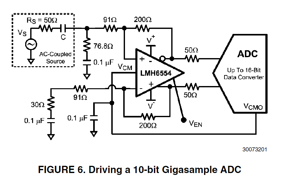
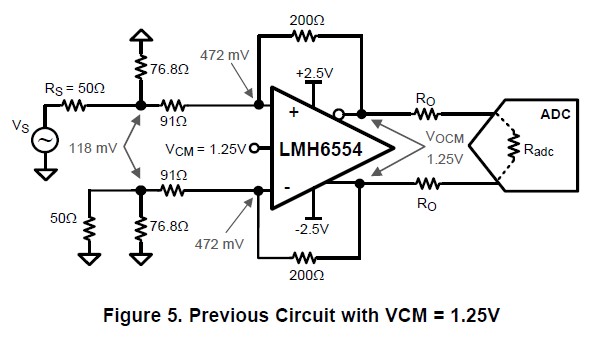
I'm working on a design consist of LMH6554 (ADC Driver) with ADC08D1000 (Ultra HS ADC). However, I realized that my signal is unable to maintain at true zero due to the offset from the feedback loop (Possible due to the VCM from ADC). Besides that, the signal is attenuated by half due to the RO resistor (50 ohms) in parrallel with the 100 ohms resistor within the ADC.

Can I know if it will be safe to remove the 50 ohms resistor without affecting the performance of the ADC?

Also, if I removed the VCM and let the ADC operated in AC-Coupled mode, will my performance of ADC be improved?

6443.LMH6554.TSC

Thanks.

  • Hi Wilson,

    If you don't "need" to process the DC component of your signal (as you are AC coupling the input), you'll get the best performance if you configure the ADC for AC couple mode. The LMH6554 VCMO pin should be at ground (with your +/-2.5V supplies).

    I noticed that your TINA schematic has an imbalance in that the un-driven input is DC coupled while the driven input is AC coupled. It is best to keep the balance, similar to Figure 6 shown here (AC couple both inputs). May be that's why you had introduced the 0.4V biasing on the un-driven input which you may not need?

    The 50ohm output resistors are there to do matching to the 100ohm differential input of the ADC and to provide LMH6554 output isolation for parasitics to the right of them. If you don't need matching (i.e. short traces and low enough frequencies compared to trace lengths), you may be able to lower the 50ohm resistors but I would keep some isolation resistance in place to keep the driver frequency response flatness. Alternatively, for larger ADC swing, you may be able to raise your gain by increasing the RF/ RG ratio (mostly by lower RG). Also, mind the input impedance in your application if you are sensitive to that?

    Hope this helps.

    Regards,

    Hooman

  • Hi Hooman,

    I have a more general question about ADC drivers...

    In our application there is a need to drive a dual ADC (as it is used to digitize I and Q of a QAM signal).

    In this case I have to use two drivers. The question is whether there is a way to estimate the I-Q imbalance presented by differences  between the two amps (I mean device production imperfection, not board related issues)?

    Regards,

    David.

  • Hi David,

    If the matching is not specified in the datasheet of the respective part, I'd say it is very difficult to try and estimate it.

    TI has dual fully differential amplifiers and some of these show the gain / phase matching between the channels. Here are some:

    Device                                  Gain Matching (dB)                        Phase Matching (deg.)                  Frequency (MHz)

    LMH6517                             +/-0.05                                              0.1                                                       150

    LMH6521                             +/-0.04                                              0.45                                                     200

    THS4522                              N/A                                                   N/A                                                        N/A

    Hope this helps.

    Regards,

    Hooman

  • The best way to get good matching between LMH6554 devices is to use precision resistors.  Using 1% resistors will not result in good matching. The Gain, CMRR and HD2 are dominated by the resistors selected for Rf and Rg. 

    When building test fixtures for this device we used 0.1% resistors.  If you use devices from adjacent positions on the tape you can often get better than specified accuracy.

  • Hi Loren,

    I'm considering to use LMH6554 to interface between a differential source with Vcm=3.5V and ADC with required input common mode of ~0.5V.

    The interface is DC coupled.

    (The supplies are about to be shifted by ~0.75V to comply with LMH6554 input common mode requirements: Vcc=~3.25V Vee=~-1.75V. So with Rf=Rg the common mode on -IN,+IN would be ~2V. Which should comply with the adjusted CMVR of 1.3+0.75=2.05V.)

    My concern is about a remark on page 5 of http://www.ti.com/lit/an/snoa565a/snoa565a.pdf:

    Which implies that a headroom for a swinging signal is required between the actual input common mode and the maximal allowed input common mode of the LMH6554?

    Does this remark apply also for a case of differential source?

    I'd expect that for balanced input the voltage on +IN and -IN pins would be equal and almost DC. So no need to keep significant headroom for swinging. Is it so?

    Thanks,

    David.

  • Hello David,

    I may be able to help and Loren may chime in later as well.

    With the conditions you have specified, the LMH6554 input pin voltage (pins 5 and 6, VICM) is dictated by the following:

    VICM= V_IN_SOURCE - (V_IN_SOURCE - VOCM) * RG / (RF + RG)

    which is just a voltage division expression.

    where in your case (assuming RF= 200, RG= 200 as an example):

    V_IN_SOURCE = 3.5V

    VOCM = 0.5V

    --> VICM= 3.5V - (3.5 - 0.5) * 200 / (200 + 200) = 2V

    That's about 1.25V headroom to Vcc which is the bare minimum required. If you raise the gain, the situation gets worse.

    The swing on the LMH6554 pins will be very small as you had also noted.

    Here is a TINA-TI simulation you can use to predict different scenarios:

    0871.LMH6554 REF Design- Diff ADC Gain Stage Hooman 3_13_14.TSC

    Regards,

    Hooman

  • David,

    Regarding the specific page 5 statement you had quoted relates to the Figure 5 schematic, shown below:

    You had written:

    "My concern is about a remark on page 5 of http://www.ti.com/lit/an/snoa565a/snoa565a.pdf:

    Which implies that a headroom for a swinging signal is required between the actual input common mode and the maximal allowed input common mode of the LMH6554?

    Does this remark apply also for a case of differential source?"

    Answer: For a differential input drive as in your case, your input pin swing will be negligible. Thus, you only need to care about VICM to make sure it is at least 1.3V below Vcc.

    In the case of Figure 5 above, having a SE input, there will be input pin swing. The VICM of 472mV leaves very little for input pin swing (828mV) before the 1.3V headroom from Vcc is violated.


    Regards,

    Hooman

  • Hi Hooman,

    Thank you for your detailed answers, they are very helpful!

    In order no to load the source with too much common mode current and present higher input impedance, I'd like to set Rg=~300, Rf=~900.

    Are there any drawbacks in using such high values?

    Thanks.

  • Hi David,

    It is possible to raise RF to 900ohm as you have noted. However, keep in mind that with a current feedback amplifier like the LMH6554, raising RF this much will significantly reduce bandwidth.

    Here is data which shows the frequency response at various feedback resistors. With RF=900ohm, the -3dB SSBW will be significantly down to only around 200MHz:

    Excel Data:

    Regards,

    Hooman

  • Hello Hooman,


    Could you please advise about the following issue with regards to LMH6554 used as ADC driver?:

    I'm using the following schematics.

    In the circuit above the specification of output voltage swing is used to avoid overloading the ADC when very large sine waves signal comes out from the demodulator.

    Basically I'm expecting the single ended output not to swing beyond Vcm+/-1.42V=0.47+1.42. Taking into account the serial resistors and the attenuator, this will translate to 0.47+/-0.48V at ADC input.

    A differential Pi attenuator was placed in case more attenuation will be needed.

    However, in addition to the differential signal at the LMH6554's output, there is a common mode spike that accompanier the differential signal. Which is problematic since it can't be dealt with the differential attenuator, and adding common mode attenuator will attenuate the Vcm=0.47V as well (which is out of ADC's spec).

    Below is a snapshot showing the one of the single ended signals (blue), the green waveform was captured using  differential probe.

    Note that the differential signal is smoothly clipped, while the SE signal includes the common mode spike that overstress the ADC.

    Can you please advise what is the reason for these common mode spikes?

    How can the be reduced, without changing the required Vcm=0.47V?

    Thanks,

    David.

  • Hi David,

    Some thoughts:

    1. Have you made sure that the LMH6554 input(s) (pins 5, and 6) do not get any closer than 1.3V to any rail (in your case the likely case would be V+ of 3.3V or 2V measured from ground) for any input / swing condition?

    CMVR is +/-1.3V typical with V+=2.5V, and V-=-2.5V:

    If you do exceed this limit, then may be the spikes are the result of the LMH6554 feedback loop trying to recover?

    In TINA-TI with your condition, I see that these inputs are sitting at 1.8V and you could possibly exceed the 2V limit with a little bit of swing.

    2. Are you sure the CM spikes you have seen are not originating from the demodulator (LTC5584)? If they originate from there, then you are the mercy of the subsequent stage (LMH6554, and its external resistors) to reject CM at the frequency of the spike. Resistor matching could also play a role here (I've not run any numbers, just a hunch).

    3. Why is the CM spike at the ADC input problematic specifically? Is it because you could be violating a voltage rating? The differential input is devoid of this, as you have shown.

    4. How are you grounding your scope when you are taking the CM waveform? Are you sure that is not an artifcat of the measurement? To avoid ground bounce from the scope probe lead ground lead, try to use the minimum length and choose a nearby point. Or, simply use a 50ohm setup driving a SMA center pin into the scope BNC terminated in 50ohm (just to be sure the spike is real).

    Regards,

    Hooman

  • Hi Hooman,

    Thank you for your response.

    I'll check in the lab the points 1. & 2.  4. you raised.

    3. The CM spikes are indeed problematic because of ADC voltage rating, which is specified relative to the Vcm level , i.e. not differentially.

    I forgot to mention an observation that can be significant:

    The spikes disappear when the Vcm is set to exactly the midpoint of the supplies, once pulled up or down by ~15mV, the common mode spikes appear. Does it provides you with any hint regarding the cause of problem?

    Thanks,

    David.

  • Hi David,

    I cannot relate your observation (disappearance of the CM spikes when Vcm is set to 0.8V or mid-rail between +3.3V and -1.7V) to anything caused by the LMH6554. My biggest suspicion is still item #1 from my 8/1/14 post (exceeding the input CM range).

    I will look for your response to the other open items to see if we can figure this out.

    Regards,

    Hooman