This thread has been locked.

If you have a related question, please click the "Ask a related question" button in the top right corner. The newly created question will be automatically linked to this question.

Output pin and VOCM pin feature of PGA280

Other Parts Discussed in Thread: PGA202, PGA280, PGA281

Hello..
I am going to measure the voltage across shunt resistance with PGA280. In order to increase the Output voltage range I am planning to use PGA202 in cascade. I am unable to understand the output pins of PGA280.The output pins are as follows:

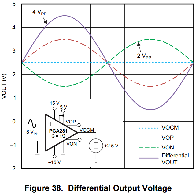
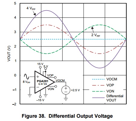
VOP: Noninverting Signal Output
VON:Inverting Signal Output
VOCM: Input,Output Common mode voltage

At which pin terminal I will get the differential output voltage ? What will be the role of VOCM and what i have to do with VOCM pin in cascade mode ?

Best Regards
Hassan.

  • Hello Hassan,

    I recommend taking a look at this reference design which details measuring the voltage across a shunt resistance with the PGA281 (same analog core as the PGA280).

    VOP and VON each output one component of the total differential output, centered around the common-mode voltage applied to VOCM. VON is a phase-inverted copy of VOP, so when they are subtracted the result is essentially 2* VOP. The idea behind the differential signaling is that twice the effective signal amplitude can be achieved while the voltage levels at each pin remain relatively low. Common-mode noise is also subtracted out, so high SNR can be achieved. The next component in the signal chain, either another amplifier or ADC, will also have a fully differential input and will perform this subtraction internally.

    Mathematically, you can consider it with the following equation:

    VOUT_differential = (VOP - VON) + VOCM
    since VON = -VOP
    VOUT_differential = 2*VOP + VOCM

    This relationship is also illustrated in the following figure from the PGA281 data sheet:

    Select VOCM to a voltage which will meet the input common-mode voltage requirements of the following stage. Keep in mind that the output stage of the PGA280 is single-supply, so a typical VOCM = 2.5V. 

    Best regards,

    Ian Williams
    Linear Applications Engineer
    Precision Analog - Op Amps

  • Dear Mr.Williams,

    Thanks for your reply. Actually in the data sheet of PGA281 page:15 Fig38 the differential output was given with Gain=1/4 so it was giving a different picture.


    As the rails of Output voltage stage are VSOP=5V and VSON=0V so our output should be in these rails. 

    Lets suppose in a scenario our DC output after multiplying with gain is 4V.
    We have:
    VOCM=2.5V
    than VOP=4.5V and VON=0.5V But when we get the differential output between VOP&VON its peak would be 6.5V. This 6.5V peak is not violating the rails limit ??

  • Hello Hassan,

    The figure in the data sheet has an error, it should be G = 1/2. 

    It's important to remember that the total differential output is not actually present at either pin. Rather, it is formed by the subtraction of (VOP - VON) that happens later in the signal chain. 

    In the example scenario above, the amplitude of the output at VOP and VON is 2Vpp, so if VOCM = 2.5V then the signal swings from 1.5V to 3.5V as indicated by the figure. This is within the output voltage swing of 40 to 100mV from the rail.

    Even if the PGA280 gain was equal to 1 and the total differential output was 8Vpp, the amplitude on VOP and VON would be 4Vpp. With VOCM = 2.5V the signal swings from 0.5V to 4.5V, which is still within the output voltage limits.

    Best regards,

    Ian Williams

  • Dear Mr.Williams,

    Thanks again for your quick response :)
    I got it if I operate the device with VSOP-VSON=5V; The maximum allowed DC output differential signal will be about ~4.8V.