This thread has been locked.

If you have a related question, please click the "Ask a related question" button in the top right corner. The newly created question will be automatically linked to this question.

PGA205AU voltage drop

Other Parts Discussed in Thread: PGA205
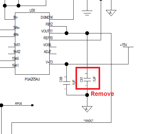
Our application used one part PGA205 INSTM AMP,SOW16. The failure has been identified Output getting 2.83V instead of 10V.
 
For more information : Pin 11(Vout) and pin 12 (FB) shorting together for getting voltage output 10VDC.
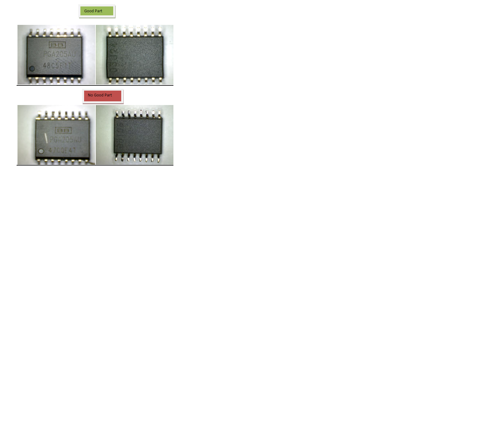
Diagnose analysis,  voltage output will be drop to 2.83V  during testing and Top surface on IC will be hot temperature . Isolate the Pin 11 and 12 (shorted) still getting 10V. re-solder back to application, measurement still getting 2.83V. We also changing with different date code of IC's, measurement of voltage getting 10V and functional testing passed. We suspect date code 47CQE4T got problem. Please discuss this issue.
  
  • Hello Ghazali,

    Please provide the following information in order for me to better assist you with this issue:

    • Complete circuit schematic
    • Expected input and output voltages and currents
    • The observed rate of failure for PGA205 in your application

    Best regards,

    Ian Williams
    Linear Applications Engineer
    Precision Analog - Op Amps

  • Hi lan,

    Thanks you for assist.

    Below information as per request. Part problem used for U30, which part voltage dropping 2.83V and top surface hot temp.

    1. Input = +5VDC and Expected Output = 10VDC (Pin 11 shorted to Pin 12).

    2. Failure rate about 9.77% ( 13/133).

  • Hello Ghazali,

    I see you have a 0.1uF capacitor on your PGA205 output. This is likely causing stability issues which could explain the overheating and incorrect DC voltage at the output. Please try removing C61 from your application circuit and test a "bad" part to see if the issue goes away.

    Best regards,

    Ian Williams

  • Hi Ian,

    For C61, designation cap for filtering the noise. This is a normal design approach and we suppose to not make any changes as this is our Customer design.

    Can you explain from the design perspective how this cap can cause IC U30  instability issue and overheating.

    Removing the cap still does not resolve the problem. All that we can do now is to change the IC with different date code to make it passed. Please explain what is the difference between these 2 date codes that inhibit different result?

  • Hello Ghazali,

    I understand the desire to filter output noise. However, the 100nF load capacitor violates the maximum stable load capacitance specification from the PGA205 data sheet. The maximum is 1000pF, or 1nF. You have connected 100x that amount.

    From a design perspective, this capacitor causes instability by interacting with the output impedance of the output amplifier to create a pole in the PGA's closed-loop response. This pole, along with the dominant pole of the PGA's output amplifier, generates approximately 180° of phase shift, reducing phase margin to nearly 0° and resulting in positive feedback. Positive feedback prevents the amplifier from correcting changes at its inputs, which gives you oscillation, high current draw, and overheating as the output transistors try to drive the oscillation to the load.

    For more information on how capacitive loads cause instability, I recommend watching our TI Precision Labs video series on stability, available here.

    If you need to meet a certain noise requirement, I can recommend an output filter with enough isolation to prevent stability issues. This usually only involves adding a series resistor at the device output pin. If you do not follow this recommendation, it's very likely that even devices with "good" date codes may have undesirable behavior over temperature or other conditions.

    Since you have removed the load capacitor and still see issues, there are several possibilities:

    • The oscillation and overheating on failed devices caused permanent damage.
    • There is still some problematic load later in the signal chain. Your schematic only shows a relay U27 and nothing after that.
    • The suspected "bad" date code does in fact have an issue.

    I recommend the following debug steps:

    • On a failed system, remove C61 as well as U27. This will disconnect all loads from the PGA205. Now monitor the output and quiescent current draw to see if they behave normally.
    • Solder a PGA205 from a "bad" date code that has NOT BEEN USED to a board with C61 and U27 removed. See if the issue is present. Try several devices to see if the issue ever presents itself.
    • If you continue to see issues from the same date code, even with no load connected, we can begin the process for failure analysis.

    Best regards,

    Ian Williams

  • Hi Ian,
    Is that possible to set this forum as private or communicate via email?
  • Hello Yeeyee,

    You can reach me via email at ian@ti.com.

    Best regards,

    Ian Williams