Other Parts Discussed in Thread: OPA1604, OPA1654
Hi,
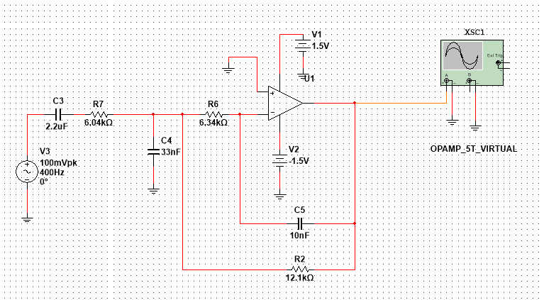
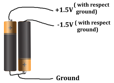
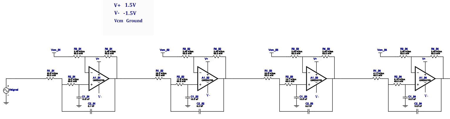
I am planning to use OPA1664 as a pre-amplifier to amplify microphone signal, using low pass sallen key topology which I have generated from TI webench. I am using dual power supply (+/- 1.5V). Microphone output is always coupled with capacitor (C3) as to avoid DC which is powering the microphone. As shown below (Fig.1)
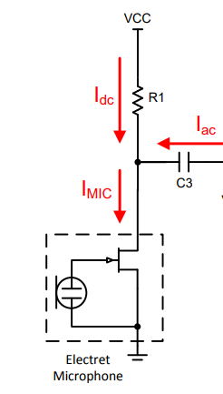
Fig.1
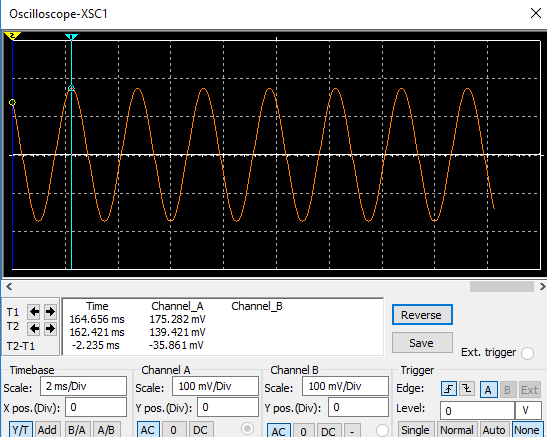
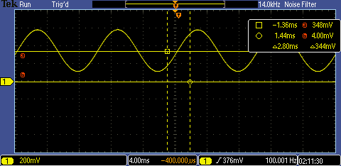
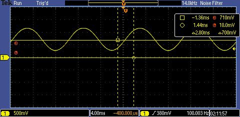
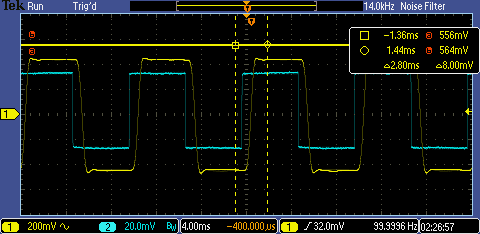
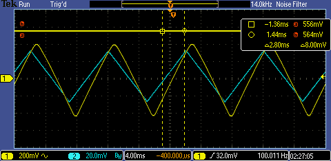
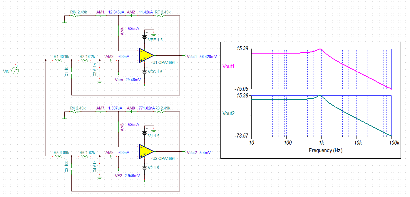
When I am doing simulation without placing the capacitor, I am getting the output as expected. Schematic and result shown below (Fig.2(a) &Fig.(b))
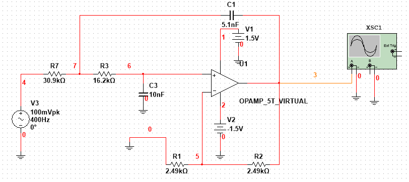
Fig.2 (a)
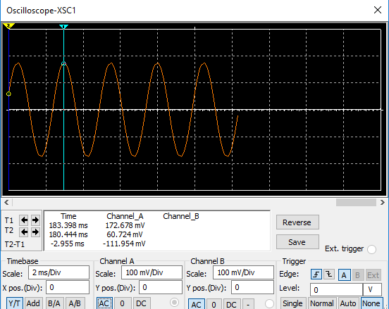
Fig. 2 (b)
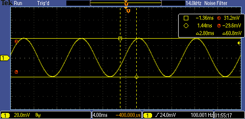
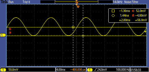
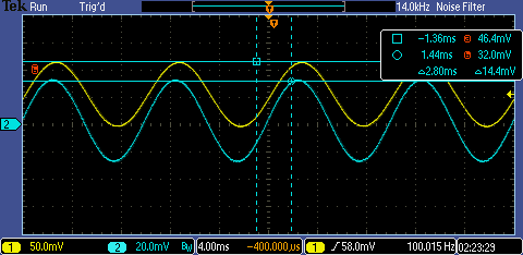
When the capacitor (c2) is placed, the output in coming in few uV instead mV as shown in (Fig.3(a) & Fig.3(b))

Fig.3 (a)

Regards,
Tapas
Fig. 3(b)