Other Parts Discussed in Thread: REF3230, OPA2364, TINA-TI, OPA364, OPA363
I am intending to use the PGA112 amplifier to measure voltages with a wide dynamic range. Peak voltage to be measured is 60 V, scaled to < 3V with a 100k / 4.7k resistor divider, and low-passed as appropriate to the application. The output of the PGA112 will then go through an output filter to the 12-bit ADC of a Piccolo or Delfino uC.
Application details: This is for sensing phase voltage in a BLDC motor controller where the controller can both be used with a wide variety of bus voltages (Vbus = 6V - 60V), and where the phase voltage will vary at 0 - 500 Hz between 0 V and duty_cycle*Vbus for 0 < duty_cycle < 1.
The application will use the gain of the PGA to adjust for changes in Vbus; for example, when running at 6V a gain of 8 will be used. However, I am not intending to change gain dynamically (between sequential readings of voltage) if at all possible. Therefore, at a given gain, the question of usable dynamic range of the PGA/ADC combination arises. Essentially, the ADC has a nominal resolution of 3.3V / 2^12 = 0.8 mV/count, but the bottom 50 mV = 62 counts are indistinguishable. If my input varies from 0V to 100 mV (very reasonable for scaled phase voltages at low duty cycle), a full half of the output is clipped and indistinguishable.
QUESTION 1: Is there a different approach I should be taking here, either with the PGA112 or a different part, to solve this problem? I considered using no amplifier gain and instead a single-ended-to-differential amplifier and the 16-bit mode of the Piccolo/Delfino ADC, but for various reasons this is not ideal.
QUESTION 2: If I continue to use the PGA112, can I set Vref to 100 mV to offet the output? I understand that this would restrict me to gains of 2+ (as Vref has no impact with gain=1), and slightly restrict my output range (from 100 mV to DVdd - 50 mV). Are there other impacts I'm missing? The datasheet discusses Vref=GND and Vref=AVdd/2 cases, but not the general case.
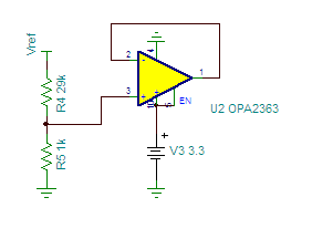
QUESTION 3: What's the most appropriate way to get a Vref in this range, with the necessary current source/sink requirements? I expect to have a REF3230 available for Vcal; should I buffer this, resistor-divide by 30, and re-buffer? Is an OPA2364 appropriate for both buffering stages here? Is it acceptable to have the output of the second buffer (the 100 mV Vref) shared by 4x PGA112s? (Output current of OPA2364 = 45 mA >> 4x PGA112 Vref current = 4*2 mA.)
QUESTION 4: Is there a PSPICE / TINA-TI model of the PGA112 available so I can answer some of these questions on my own?