Ian Williams (high-speed amplifier applications engineer) says:
Answer:
Yes, it is perfectly acceptable to power these devices with a -12V rail at -Vs and GND at +Vs. The device only cares that the total voltage across its supply pins is within the range given on the data sheet. However, you must take care to bias the input signals properly since the mid-supply point will be -6V.
The THS4211 and OPA2691 devices can swing within 1V of their supply rails, so that means a -1V to -11V swing with a single -12 volt supply. Below is a scope capture of the THS4211 swinging to +/-5V output with a +/-6V supply and R_L = 100ohms. The TINA simulation results of the OPA2691 with Vs = +/-6V are also below, which shows the device swinging to just under 1V below the rails.

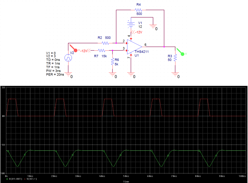
Following is an example of how to bias the output at -6V, or mid-supply, to allow for the greatest output voltage swing.
Let's assume that the input signal is a pulse that transitions from 0V to
3V. We know we can't violate the input common mode voltage of the
device, so to handle this input range we will place a bias voltage on
the non-inverting input. In the circuit below, we have taken the -12V from
the negative supply and used a simple resistor divider to bias the
non-inverting input at -3V. Since the amplifier wants to keep the
voltage at both input pins the same, that will cause a -3V bias voltage
on the inverting pin as well. In this example circuit we simply have a DC
voltage of 0V being applied, so the voltage difference across R2 (Rg) is
3V, inducing a 6mA current (3V/500ohms = 6mA). Since that current can't
flow into the high-impedance input pin, it flows through R4 (Rf), which
causes another 3V drop that results in -6V at the output node. To be
more correct, the 6mA current originates at the amplifier output and
flows back through the feedback network and then through Rg and the
input source.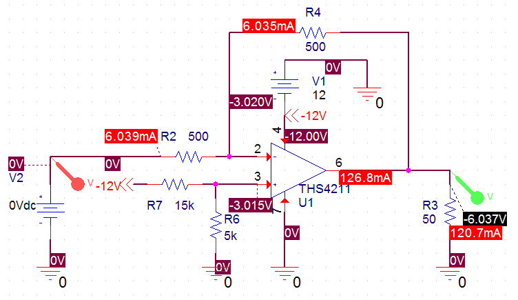
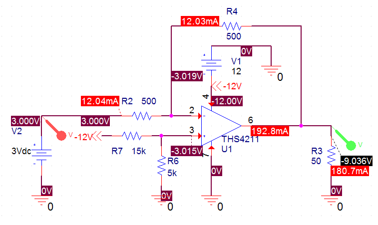
If we instead have a 3V DC input signal, the same analysis can be used except in this case the voltage difference across R2 is 6V, inducing a 12mA current. The 12mA current through R4 causes another 6V drop which results in -9V at the output.
Here's the circuit with the 0 - 3V input pulse applied. We changed Rf and Rg to 500 ohms to stay closer to the standard G = -1 values on the THS4211 data sheet. You can see the output transitioning from -6 to -9V as the input transitions from 0 to 3V. However, since the input has a slew rate of 3V/1ns = 3000V/us, the amplifier lags behind since its typical slew rate is 970V/us. A part such as the OPA690 would do better with the faster input pulse.