This thread has been locked.
If you have a related question, please click the "Ask a related question" button in the top right corner. The newly created question will be automatically linked to this question.
Hi,
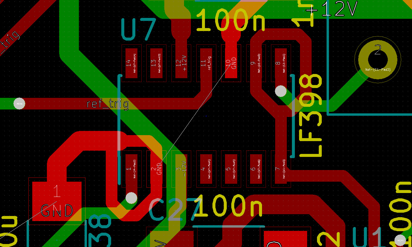
I'm using the LF398 sample and hold circuit for an acquisition chain and it's time for PCB layouting.
LF398 datasheet talks about guarding ring around input pin for the TO-99 package. Is it also doable with the SOIC package, around the input pin 1 thanks to pin 2 'NC' ? Or must the NCs pins not be connected?
Also, if no offset adjustment is needed, should the 'Offset adjust' pin be grounded, or floating (as we can see in this thread https://e2e.ti.com/support/amplifiers/etc_amplifiers__other_linear/f/18/t/450655?tisearch=e2e-quicksearch&keymatch=LF398 ) ?
Thanks
Alexis
Hello Alexis,
The LF398 14-pin SOIC package can be configured in a similar manner to the TO-99 version that incorporates a guard ring. A guard ring can be created by extending the pin 7 output pin trace to where it encircles pin 8 the CH pin, forming a guard ring around it. Pin 8 would have a short, separate trace to which CH connects on one end. The guard ring trace could connect to pin 9 without creating any issues because it is a No Connect - NC pin. NC pins do not make connections to anything internal to the IC.
If you do not wish to use the Offset Adjust function provided by pin 14 simple leave that pin open.
Regards, Thomas
Precision Amplifiers Applications Engineering
Hi Alexis,
The LF398-N input bias current to pin 1 isn't particularly low; 100 nA max over temperature so having the guard ring isn't as critcal as when the input current is very low. However, it doesn't hurt anything having it in place around pin 1 and I wouldn't change the layout you have made. The execution of the guard ring around pin 8 looks very good. Here the goal is to minimize leakage current from the CH capacitor and guarding is a good idea.
Muy bueno!
Regards, Thomas
Precision Amplifiers Applications Engineering