Other Parts Discussed in Thread: INA260, TIDA-00614
What are the layout recommendations for and internal shunt resistor current sense amplifier.
This thread has been locked.
If you have a related question, please click the "Ask a related question" button in the top right corner. The newly created question will be automatically linked to this question.
What are the layout recommendations for and internal shunt resistor current sense amplifier.
Sourcing or sinking high current through a resistive path is going to generate heat; dissipating that heat is a fairly common challenge engineers encounter. With internal shunt products like the INA250 and INA260, wherein a physical shunt resistor is placed inside a package along with an amplifier, certain considerations should be taken regarding the layout around the IC. Note that one significant benefit of using an integrated shunt current sense amplifier is that with the shunt in the package with the amplifier, the two components drift together, creating a condition where gain error is much more stable and predictable. The temperature coefficient of the INA250 from 0°C to 125°C is just 10 ppm/°C.
| Approximate physical layout inside the package of the INA250 |
 |
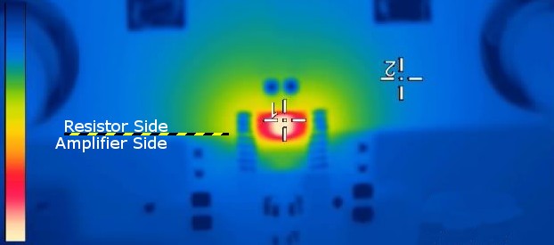
| Thermal image of the heat generated as sustained high current flows through the INA250 |
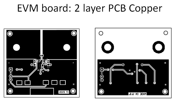
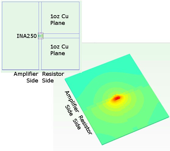
One practical method for removing heat from a device on a circuitboard is to increase the surface area of a heat-conductive metal directly in contact with the device. It is common to see large metal heat sinks attached to microprocessors and MOSFETs for power applications. In this case, using the circuitboard itself as a heat sink is appropriate as the leads of the internal shunt product (like the INA250 and INA260) are metal and provide the best direct access to the resistive element (in this case, a shunt resistor). Lay out the board with large planes attached to the shunt resistor leads of the INA250 or INA260 to promote heat dissipation away from the package and then through convection away from the PCB by exposing this large metal surface area to the surrounding air.
 |
| Layout of a general purpose INA250 PCB evaluation module |
Increasing the weight of the copper on the board will also provide some benefit, both in carrying higher currents on PCBs and in heat dissipation. 1oz, 2oz, and 3oz copper are common weights to choose from for PCBs. Increased copper weight may also mean that you need to consider ICs with a wider pitch between the leads to accommodate the thicker copper traces and pours.
 |
| Thermal modeling of heat dissipating away from the INA250 |
Convection is the second important factor in heat dissipation. If the PCB is enclosed, then the heat may not be able to escape as the ambient temperature of the air around the PCB rises. Including vents and fans in your application can promote airflow to move the heat away from the device and PCB. TIDA-00614 shows how an INA250 solution temperature can rise over time with different currents, both with a fan and without in the figures below (figures 10 and 11 of the design guide).
| TIDA-00614: General purpose EVM Layout modified to have two INA250 devices in parallel, increasing the maximum sustained current capacity to 30 A |