This thread has been locked.
If you have a related question, please click the "Ask a related question" button in the top right corner. The newly created question will be automatically linked to this question.
Hello all,
my question is closely related to https://e2e.ti.com/support/amplifiers/f/14/t/177561
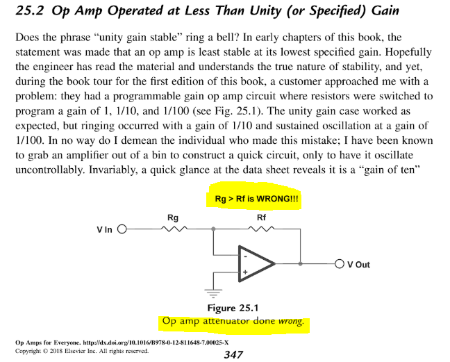
The issue there was to use an operational amplifier as attenuator (e.g., to convert an input voltage from 0..10 V to 0..2.5 V). As solution, a voltage divider to bring down the input voltage followed by a (unity-gain) buffer was suggested. This seems in line with what the book "Op Amps for Everyone" (by Carter, Mancini) suggests. The book explicitly warns not to use an inverting opamp as attenuator:
However, I've seen this configuration (0 < |G| < 1) suggested several times (e.g., on electronics stackexchange here). Additionally, I've read discussions where people contest Mancini's statement. They are saying that a non-inverting gain of 1 is the worst-case for op amp feedback stability, which is equivalent to an inverting gain of zero. They conclude that if the OpAmp is specified to be stable at unity-gain buffer configuration, it should be stable at less than unity gain in an inverting configuration, too.
Coming back to the original issue, what's wrong with this solution to the question (except that the output is "inverted"), using an inverting OpAmp as attenuator:
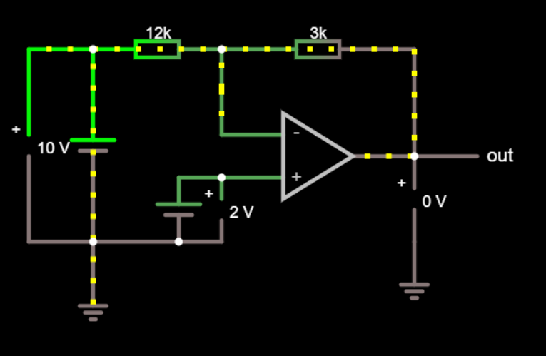
This is the link to the simulation.
Thanks!
Morning folks,
This actually was a classic mistake by Bruce Carter that Mancini seems to paper over for some reason. Somewhere Bruce got the idea that an inverting configuration had a noise gain of Rf/Rg instead of the correct 1+Rf/Rg. Bruce Trump and I wasted about an hour one day trying to explain that error to him with no luck.
If the op amp itself is unity gain stable, inverting attenuators will be stable. You can get into phase margin problems with faster parts using higher R values due to the pole in the feedback back to the inverting summing junction parasitic C. Since attenuators were so common with FDA's (taking higher swing signals down to an ADC input range), I added that as section 9.1.6 in the THS4551 datasheet. There, I used the noise gain shaping technique using capacitors from this recently rebuilt 1997 article
Hi Kai and Michael,
Thank you for all the help!
Hi Daniel,
Just to quickly summarize Kai and Michael's responses, there is no issue with designing an inverting attenuating circuit as long as the amplifier does not require a noise gain (non-inverting gain) greater than 2V/V.
Our TI Precision Lab videos on Bandwidth might help explain why some amplifiers are not unity gain stable.
Thank you,
Tim Claycomb
Hi Kai,
kai klaas69 said:
you omit the crucial point of Ron Mancini's explanation, that the discussed OPAmp is only "gain of ten" stable! ...
To me, Rom Mancini's advice does not read as it is limited to the discussed OpAmp. Rather it sounds like a general advice for OpAmp circuit design.
This understanding seems to be supported by the discussion in his book in the chapter about OpAmp theory: it asserts that in general "gains less than unity become unstable".
I have to say that I find the highlighted statement inconsistent with the claim "unity gain is being the LEAST stable operation point of the op amp".
I don't know what your circuit shall do, but the -input of OPAmp will sit on a +2V offset. So, the input signal current will not flow into virtual ground (0V) but into a virtual +2V potential. Is this what you want?
It should convert the input voltage range 0..10V to the output voltage range 2.5 .. 0 V. That's what the circuit is doing according to the simulation. Why do you say that the -input "sit on a +2V offset" when the +2V bias is connected to the +input of the OpAmp?
Thanks.
Dan
Funny, that we both came across the same discussion...see the link in my original posting. ;-) Sometimes the Internet is just like a small village.Michael Steffes said:There was actually an amusing flare up on this one some years back ...
forum.allaboutcircuits.com/.../
Yea Daniel, In some ways it was hilarious that Carter was locked into this idea. Treat the signal gain and then noise gain as two issues. Also, I took another run at VFA loop gain stability in this article
www.planetanalog.com/author.asp
Where the leadup one was maybe more interesting - here, fig. 4 explains why Gain Bandwidth Product often does not work to predict SSBW. That is another one folks get very confused about. That was a job and a half. It does work fairly well until you get into higher order Aol poles out in frequency - Which is common in higher F parts. I was using this also for the next one using CFA and those plots 2&4 in Insight #5 work very well there as well.
www.planetanalog.com/author.asp
Hi Michael,
if the "programmable gain OPAmp circuit" used switched Rf resistors, then it's possible that the analog switches added some undesired stray capacitance from the -input of OPAmp to signal ground. This could have added phase lag in the feedback loop and eroded the phase margin.
Kai