This thread has been locked.

If you have a related question, please click the "Ask a related question" button in the top right corner. The newly created question will be automatically linked to this question.

OPA552: Getting noise in part of a generated wave

Part Number: OPA552
Other Parts Discussed in Thread: DAC8806,

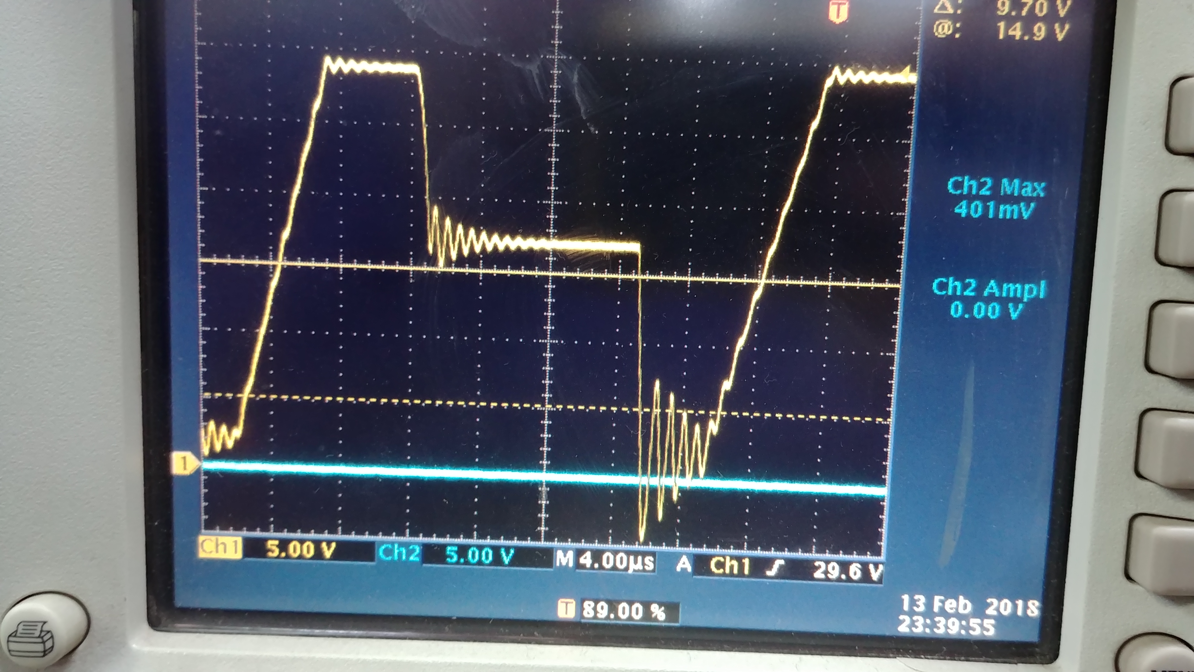
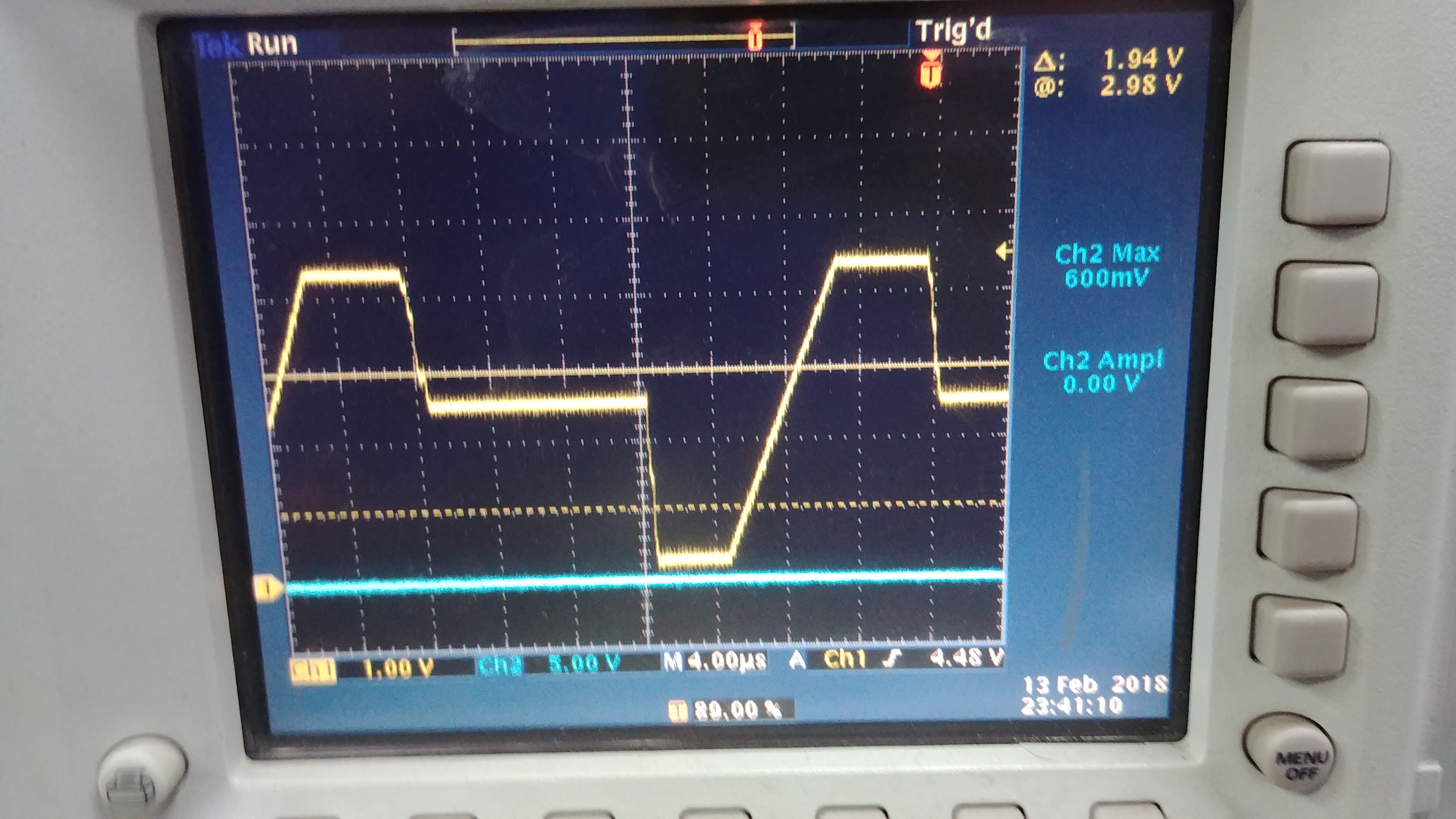
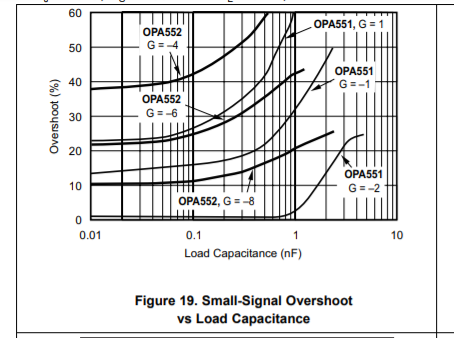
Hi, I am generating a square wave using the DAC8806. I am then driving a 4011 opamp that then drives the OPA552.  In front of the opamp, the signal looks clean. The OPA552 uses a resistor gain ratio to give a 6x gain. The power rails are -9v and +41v.  The DAC has a refresh time of 200ns. At ~2000ns, the square wave is clean. What can I do to get a cleaner wave? I am currently driving a 50fp CAP with the OPA552 in an effort to clean the signal. I also ordered some opa551s today. Do you have any suggestions on how to get a cleaner wave. The jitter you see is about 1us or 1MHz. The pictures are before and after the OPA552. In TINA, I could not make this noise.dac8820 positive only 30v peakB.TSC - TINA.pdf

  • Morning Doug, 

    Those waveforms are indicative of low phase margin,can you post the exact circuit - TINA file would be better. 

  • 1411.dac8820 positive only 30v peakB.TSCI added a TINA file and a pdf in the original post

  • Thanks Doug, that makes it easy,

    Very likely your feedback and gain R are too large and causing a loop pole with the capacitance on the inverting node. I tried LG phase margin sim and it shows 48deg, not bad - but if the input C was actually higher than the datasheet, would degrade rapidly. I have not checked what input C is in the model (the next Planet Analog article), just used the spec lines in the LG sim. 

    Above, you say your cap load is 50fF?? Sure you don't mean 50pF?

    If I add that to the LG sim, it drops down to 33deg.

    I would try dropping your Rf and R2 down by a factor of 10, should fix this unless it is a load issue - and I don't see any load yet.

    OPA552 stability.docx

    OPA552 LG updated.TSC

  • Michael, I will try dropping the resistors down by a decade. Thank you very much. I will keep you posted on my results. I should know by tomorrow.
  • Hi Doug,

    Michael is right on the mark; this is a low phase margin issue. That very large ripple especially evident with the second pulse in the upper image, having almost 5 V overshoot would indicate a phase margin of about 35 %. At least that is what the "Figure 47: Stability - Phase Margin vs. Percent Overshoot" graph indicates in TI's Analog Engineer's Pocket Reference. That is line with Michael's assessment. You can find the pocket reference here:

    This overshoot, ringing behavior result can be had as the result of the load capacitance applied to the output of the OPA552 acting in conjunction  with the OPA552 open-loop output impedance (Zo). You indicated that your output load capacitance is 50 fF, or possibly 50 pF, but you haven't mentioned the capacitance of the cable or probe connecting the OPA552 output to the O-scope. That certainly adds to the 50 xF capacitance connected to the output. The datasheet table shown here provides a good indication of the OPA552 C-load capability, and associated % overshoot.

    Note that this is small-signal behavior and your signals are large-signal by their level. Therefore, slew rate enters into the overall transient response. However, in a Gain of +6.6 V/V you are using it is evident that the OPA552 will have significant overshoot with less than 100 pF.

    Additionally, the phase margin is reduced somewhat by the pole created within the feedback loop, by the op amp feedback resistor and op amp input capacitance. You are using a 56 k RF, and 10 k RI. Reduce their values by a factor of 10x, and see if that helps reduce the ringing.

    Regards, Thomas

    Precision Amplifiers Applications Engineering